- 23 -
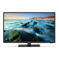
LCD TV Service Manual
Hisense Confidential
4. Circuit instruction
4.1 Power assign and block diagram
Power assign:
Power voltage includes 12V_M、5V_M、5VS and VPA(Voltage Power for Audio, normally
14~16V),some small size TV’s( small than 37 inch) VPA will use 12V_M directly .All other
voltages are converted from the above voltages.
a. 5V_TUNER that power supply for Tuner is converted by U9 from 12_M; The power supply
for panel is converted by chosen output between U31 from 12_M and 5V_M ;The power
supply for the audio IC (U35) of small size TVs is converted by the output of 12V_M connects
ferrite bead and VPA;the last, the 33V rising circuit and mute circuit are converted by the 12_M
directly.
b. Both of the 5VM and 5VS pass through diodes then output 5V_ON,which used for
3.3V/1.2V/DV10 convertion. U36(DAC)、U29/U30(audio switch)、U7(DAC)、U19(IF )
and USB are converted from 5V_M directly ;The power supply for DDR(U1,2.6V) is
converted by U11 from 5V_M too
c. 3.3V supply for U17(FLASH),U14(EEPROM)is converted by U4 from 5V_ON . 1.0V supply
for U34(the main IC \MT8222)is converted by U3 from the 3.3V ; 1.2V power supply for the
main IC \MT8222. is converted by the 3.3V
 Loading...