5.
4
POWER
SOURCE
CIRCUIT
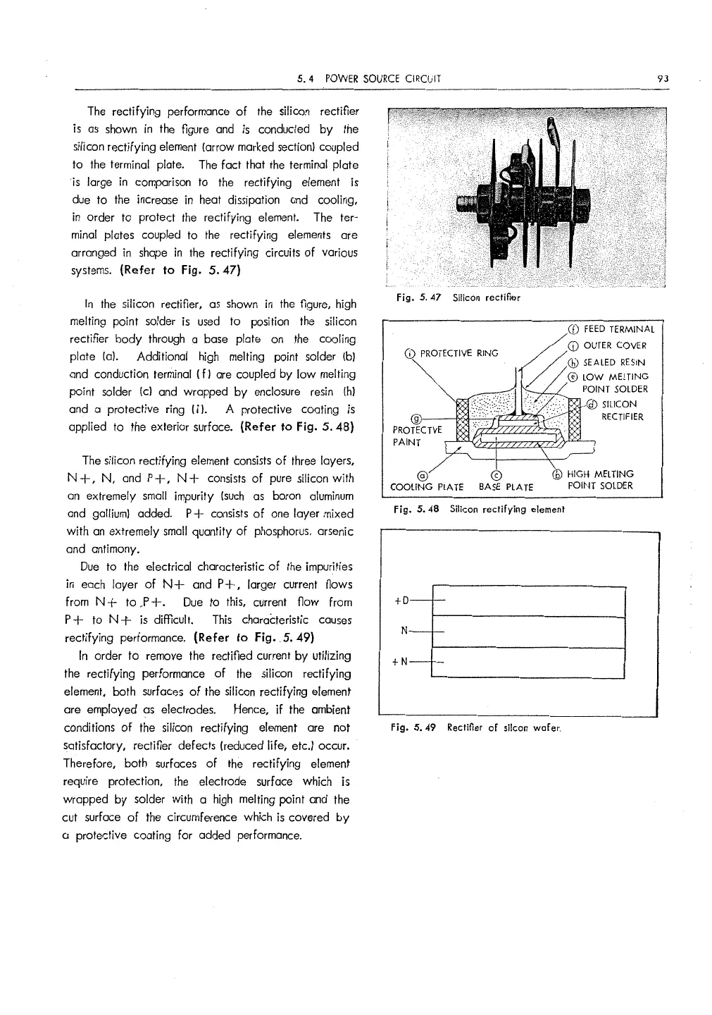
The rectifying performance
of
the silicon rectifier
is
as
shown in the figure and is conducted
by
the
silicon rectifying element (arrow marked section} coupled
to
the terminal plate. The fact that the terminal plate
is
large
in
comparison to the rectifying element is
due to the increase in heat dissipation and cooling,
in
order to protect the rectifying element. The ter-
minal plates coupled to the rectifying elements are
arranged
in
shape
in
the rectifying circuits
of
various
systems.
{Refer to
Fig.
5. 47)
In
the silicon rectifier,
as
shown
in
the figure, high
melting point solder
is
used
to
position the silicon
rectifier
body
through a base plate on the cooling
plate (a). Additional high melting point solder {bl
and conduction terminal
(fl
are coupled
by
low
melting
point solder
(cl
and wrapped
by
enclosure
resin
{h)
and a protective ring ( i
l.
A protective coating
is
applied to the exterior surface. (Refer to
Fig.
5. 48}
The silicon rectifying element consists
of
three layers,
N
+,
N,
and P
+,
N + consists
of
pure silicon
with
an
extremely
small
impurity
(such
as
boron
aluminum
and gallium} added. P + consists
of
one layer mixed
with
an
extremely
small
quantity
of
phosphorus. arsenic
and antimony.
Due
to the electrical characteristic
of
the impurities
in each layer
of
N + and P
+,
larger current flows
from N
+ to
,P
+.
Due
to this, current
flow
from
P
+
to
N + is difficult.
This
characteristic
causes
rectifying performance. (Refer to
Fig
. . 5. 49)
In
order
to
remove the rectified current
by
utilizing
the rectifying performance
of
the silicon rectifying
element, both surfaces
of
the
silicon rectifying element
are employed
as
electrodes. Hence,
if
the ambient
conditions
of
the silicon rectifying element are
not
satisfactory, rectifier defects (reduced life, etc.} occur.
Therefore, both surfaces
of
the
rectifying element
require protection, the electrode surface which is
wrapped
by
solder with a
high
melting paint and the
cut surface
of
the circumference which
is
covered
by
a prote,:;tive coating
for
added performance.
Fig.
5.
47
Silicon rectifier
~'""NC
®
PROTEC
TYE
PAINT
(0
FEED
TERMINAL
CD
OUTER
COVER
½
Cb)
SEALED
RESIN
@ LOW MELTING
.
POINT
SOLDER
@
SILICON
RECTIFIER
@ @ @
HIGH
MEL
TING
COOLING
PLATE
BASE
PLATE
POINT
SOLDER
Fig. 5.
48
Silicon rectifying element
+D--
N-c-
+N--
Fig. 5. 49 Rectifier
of
silcon wafer.
93


 To Next Page