Sect.
III
Page 3
reference. When V3B conducts the Bi-Stable Unit
is
flipped back to its original state, completing one
cycle of operation.
Voltage regulator tubes V5 and V6 are connected
by a voltage divider from which the switching refer-
ence voltages are taken. They also provide the
limiting voltages applied to tubes
V7 and V8 which
are seen to be a push-pull clamping system. In-
asmuch as the integrator output
is
directly related
to the input, it
is
seen that the magnitude of square-
wave applied must be carefully controlled. Al-
though only the squarewave appearing at the plate
of Vl
is
needed to drive the integrator, the clamp
is
made push-pull to prevent excessive current
variations in the regulator tubes. The action of
V7B and V8B
is
such that if the applied waveform
has peak excursions in excess of the potentials on
the remaining cathode and plate, these being deter-
mined
by
regulator tubes V5 and V6, a current will
flow through R20 which drops the voltage to very
nearly the potential of the regulated element of the
conducting section of the diode. The action of the
other diodes
is
the same, but 180" out of phase,
inasmuch as they are coupled to the plate of V2.
In
this way, waveforms appearing on the clamped
sides of R21 and
R20 are assured to be of equal
magnitude as well as
180" out of phase, and further
the average of dc level of the squarewave
is
ac-
curately controlled.
3-3
LINEAR INTEGRATOR
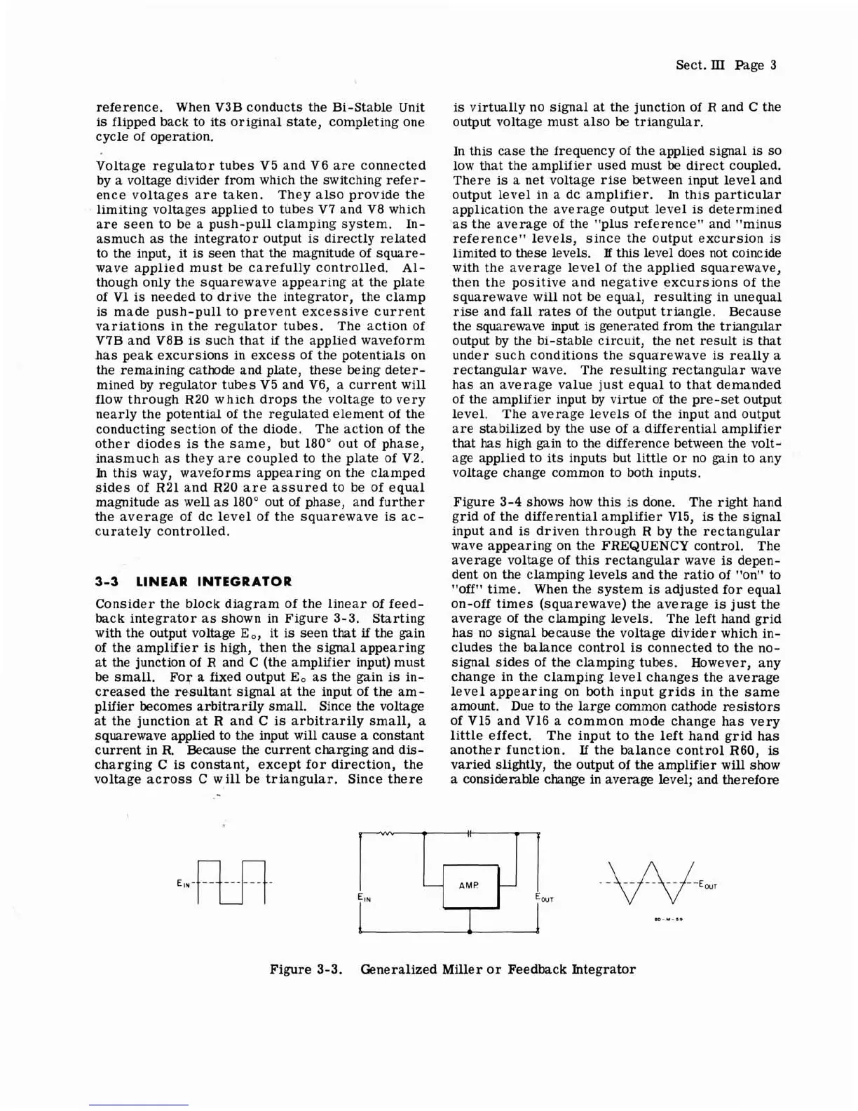
Consider the block diagram of the linear of feed-
back integrator as shown in Figure 3-3. Starting
with the output voltage
E,,
it
is
seen that
if
the gain
of the amplifier
is
high, then the signal appearing
at the junction of R and
C
(the amplifier input) must
be
small. For a fixed output Eo as the gain
is
in-
creased the resultant signal at the input of the am-
plifier becomes arbitrarily small. Since the voltage
at the junction at R and
C
is
arbitrarily small, a
squarewave applied to the input will cause a constant
current in R. Because the current charging and dis-
charging C
is
constant, except for direction, the
voltage across C will be triangular. Since there
is
virtually no signal at the junction of R and C the
output voltage must also be triangular.
In this case the frequency of the applied
signal
is
so
low that the amplifier used must be direct coupled.
There
is
a net voltage rise between input level and
output level in a dc amplifier. In this particular
application the average output level
is
determined
as the average of the "plus reference" and "minus
reference" levels, since the output excursion
is
limited to these levels.
B
this
level does not coincide
with the average level of the applied squarewave,
then the positive and negative excursions of the
squarewave will not be equal,
resulting in unequal
rise and fall rates of the output triangle. Because
the
squarewave input
is
generated from the triangular
output by the bi-stable circuit, the net result is that
under such conditions the squarewave
is
really a
rectangular wave. The resulting rectangular wave
has an average value just equal to that demanded
of the amplifier input
by
virtue of the pre-set output
level. The average levels of the input and output
are stabilized by the use of a differential amplifier
that has high gain to the difference between the volt-
age applied to its inputs but little or no gain to any
voltage change common to both inputs.
Figure 3-4 shows how this
is
done.
The right hand
grid of the differential amplifier
V15,
is
the signal
input and
is
driven through R by the rectangular
wave appearing on the FREQUENCY control.
The
average voltage of this rectangular wave
is
depen-
dent on the clamping levels and the ratio of "on" to
"off" time. When the system
is
adjusted for equal
on-off times (squarewave) the average
is
just the
average of the clamping levels. The left hand grid
has no signal because the voltage divider which in-
cludes the balance control
is
connected to the no-
signal sides of the clamping tubes. However, any
change in the clamping level changes the average
level appearing on both input grids in the same
amount. Due to the large common cathode resistors
of V15 and V16 a common mode change has very
little effect. The input to the left hand grid has
another function.
If
the balance control R60,
is
varied slightly, the output of the amplifier will show
a
considerable change in average level; and therefore
Figure 3-3. Generalized Miller or Feedback Integrator
-
-
-
-
€9,
Eour
ID-"-5.
AMP
t
a
-