Sect.
111
Page 6
The
sinewave
is
approximated by varying the shunt
resistance across
R93B
is
steps determined by the
diode synthesizing network. The waveform slope,
at first,
is
just that determined by R94, R93B and
the input waveform. When the first diode conducts
R93
is
shunted by a predetermined amount, decreas-
ing the slope. Each diode in turn decreases the
slope until all the diodes are conducting and the
triangular wave
has
reached
its
crest. The triangular
wave starts down, the diodes stop conducting in turn
until the triangular wave has reached its crest. The
triangular wave
starts
down, the diodes stop conduct-
ing in turn until the triangular wave reaches the
average level. The other half-cycle is formed in
the same manner, but by the diodes that are biased
to shape the negative excursion.
It can
be
shown that using seven segments to approx-
imate one half cycle of the
sinewave results in ap-
proximately 11 6% rms distortion. However, variations
in the diodes limit the practical result to about
1%
rms distortion.
In
the triangular wave position of the FUNCTION
selector switch the non-linear load consisting of
the diode network
is
replaced by R95 so that the
combination R94 and R95
is
a simple linear divider
for all voltage levels. It
is
adjusted to give equal
sine and triangular wave peak magnitude.
The
squarewave
is
connected to the FUNCTION selector
switch through the divider R59 and R22 which adjusts
the average voltage of the squarewave to the voltage
at the cathode of V4. In the squarewave position
of the selector switch, R63 parallels
R93B to adjust
the amplitude of the squarewave to be equal to the
amplitude of the
sinewave and the triangular wave.
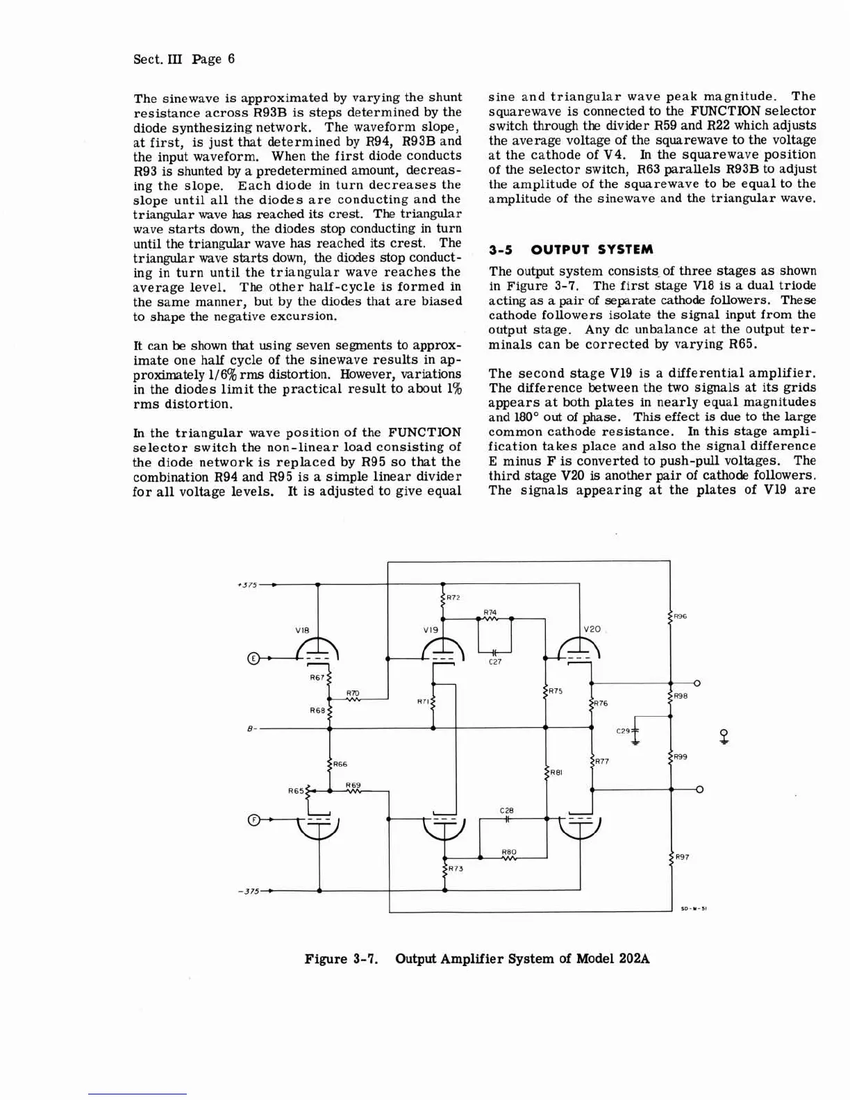
3-5
OUTPUT
SYSTEM
The output system consists of three stages as shown
in Figure 3-7. The first Stage V18
is
a dual triode
acting
as
a pair of separate cathode followers.
These
cathode followers isolate the signal input from the
output stage. Any dc unbalance at the output ter-
minals can be corrected by varying R65.
The second stage
V19
is
a differential amplifier.
The difference between the two signals at its grids
appears at both plates in nearly equal magnitudes
and 180" out of phase. This effect
is
due to the large
common cathode resistance. In this stage ampli-
fication takes place and also the signal difference
E
minus F
is
converted to push-pull voltages. The
third stage V20
is
another pair of cathode followers.
The signals appearing at the plates of
V19 are
Figure
3-7.
Output Amplifier System of Model
202A