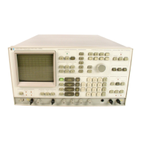
Model
-15
75 A
tlut trigger
the
J-K ilip
flops decreases until a
point
is
reached
where
the
trausitiorl rcgiolis overlap. L) the case
rvhere
A rnd
Bare
l80degreesoul ofphase, Agoeshighat
the sJnre tirne B
goes
low; thus,
A and B'occur stnulta-
neousl!.
Sii'.rp the Pl flip
ilop (lC7A)
is
"sct"
by A and
"resct'
b)' B'. it could not respond
properly.
The same
is
true
1'or
the PJ
llip flop
since it is controlled by the other
two transitior)s,
A'and
Il. Due
to the
fixed response
tirne
of
the
J-K 1)ip
flops. they will
respond
to a mlL\irnurn
phase
diffcrcnc,-' of 150 dcgccs at l0 \lHr and approximatcly
175 degrees ut
I \lHz. In order
to accurately
mcasure
phase
in this region. it is neoessary to invert the signal on one
channel so that thc
phase
differerce
is within
the operating
rangc of the
J-K
l1ip flops. Tlris is accomplished by rneans
of
thc
"Q"
Pllasc Dctcctor rvhich scnscs thc
phasc
nragrlitude
and
inverts
thc
output of thc B channel
Exclusive OR
gate
whell the
phase
rnagnitudc
is
greater
tlran
90
degrees.
4-30.
"0"
Phase Detector
(Schematic
No
s.2,3 and
4).
:1--ll.
Reler lo thc Functional Block I)iagrant
(Figure
7-l
)
lir the
loLl,livirg
d is:ussion.
.1-.11.
The
'Q'
Phase Deteclor is cornprised oi one Exclu-
sive OR
gule.
a
Diffcrential
Amplifier, a Corstant Currcnt
Source
antl
a BLrffcr,/lntegrator. Thc output of the Bufler/
Iutegrator is fil{ered b}' the l'>hase
Control
Filter
(A7)
and
applied to a Threshold Detector. The Threshold Detector
provides
a
high (l) oL low
(0)
eutput depending on
the
magnitudc of tlie
phase
diflbrence between
the two input
signais.
\\1lell
lhe
phase
rnagritude is less than 90 degrees,
the ThreshoLd
L)etector
output
(designated
"Q")
is high:
ivhen the
phase
nlaglitudc is
greater
than
90
degrees,
the
output is
low.
Tlrc
"Q"
output is applied to the B cha|nel
Lrclusive OII
gatc
where
it
is used
to invert the
Exclusive
OR output rvhel] the
phase
nragnitude is
geater
than 90
degrees. The
'Q"
output
is
also applied to the Phase
Cortrol l-ogic
to cnrblc iogic circuits
tlut
control the X
and
Y
current
siIks.
.1--l-1.
The two signals applied to the Exclusive OR
gate
in
t lrc
O'Ph,.c
l)cle.t,,r Jrc A arLl 86'.
llre
output ofrhe
I rilu.iru
Ol(
jJr(
{J(\i:'r,rr(J
Pll i} hiEI
11.1
nlrcrr A'rnd
Ild
iire in opposi{e states
(one high, one lorv)and loiv
(0.1
rvhen
llrel are
in
identicxl states
(both
high.
both loiv). The
wjdth ol llre
outpul pulscs.
thereforc. reprcsents the
rlragritude ol-tirc
phase
difference between the two signals.
The
L-xclusive
OR orLtput is
applied to a
Differential
Arnplifier
ivhich
provides
the voltage swing required to
gate
oD and
gate
off the
Constaot Current Source. The
pulsating
dc lionr
the Constant Current Source is applicd to the
Bullir/i Irtcsrator which. likc
the Buffer/lntegrator in the
Phase lleleclor. serves
as an inrpedance converter. an
ilverter
and
high frequencl, integrator.
The
output of
the
Buifsr/lntcgrutor is applied to lhc Phasc
Control
Filter
which
detects
thc average value o[
the
pulse
train and
provides
a dc
output voltage proportional
to
phase
magni-
tudc.
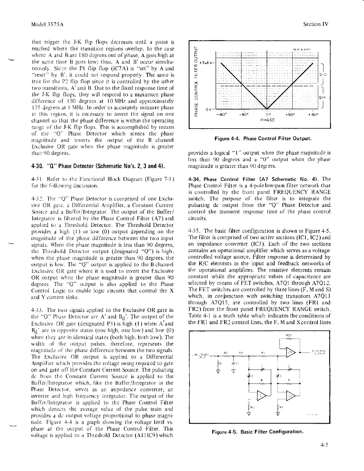
Figure 4-'1 is a
graph
showing the
voltage level
ys.
phdse
at the output of thc Phasc
Control
Filter.
This
voltage
is applied
to
a Threshold Detector
(Al
I lC9) which
't
C=0
)
l
)
)
F
o
+3.6v
I
ii
z
<
ov
-rao"
_90.
oo +9o" +
80"
PHASE
\
Figure
4-4. Phase Control
Filter
Output.
provides
a
logical
"1"
outpul when the
phase nlagnitude is
less
than 90 degrees and a "0"
output when the
phase
rrtrgnitude i:
gre3lJr
tlrJI
')O
deJ.'es.
4'34. Phase Control Filter
(A7
Schematic No. 4).
The
I'hase
Control
Filter
is
a 4-polelow-pas
filter network that
is controlled by the front
panel
FRF-QUENCY RANCE
switch. The
purpose
of the lllter i-s to integrate the
pulsating
dc output
liorl the
"Q"
Phase Detector and
control
the transicnt
rcsponse tinre of the
phase
control
circuits-
.1'35.
The basic
filter
configuration is
dlown in Figure 4-5.
Tlle filter
is corllprised of two active sec tions
(lC
I
,
IC2)
and
aII in]pedance
converter
(lC3).
Lach of the two sections
cortains an operational anrplilier which
serves as a
voltage-
controllcd voltage
source. F ter
response
is determined by
the R/C elements in the input and
feedback
networks of
the operatiorEl
amplifiers. The
resistive elements
remain
constant
wtrile the appropriate values of capacitance
are
selectcd by nrearrs oI FET
srvitches, ATQI tlrrough A7Ql2.
Thc FDT
switches are controlled by th(ee
lines (F,
M and S)
rvhich. in conjunction with
switching
transistors
A7Q13
through
A7Ql5, are controlled by two lines
(FRl
and
FR2) from the
front panel
FREQUENCY RANGE
switch.
Table
.1"1
is a truth table which indicates the conditions of
the FR1 and FRI control lines- the F. M and S control lines
Section
[V
f;'
Figure
4-5. Basic
Filter Conliguration.
4-5
 Loading...