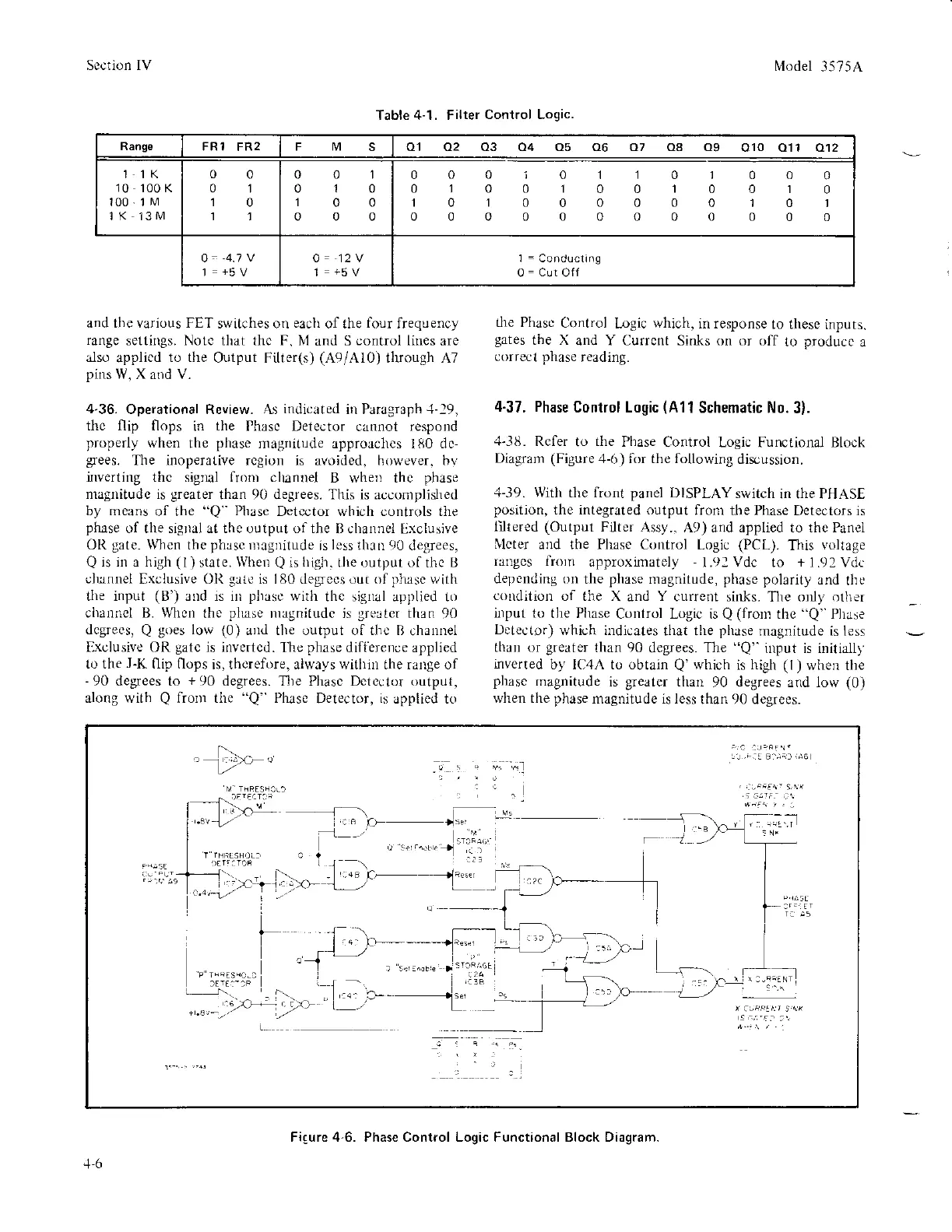
Range
FR1
FR2
Ft\4S
o1 a2 o3 o4 o5 o6 a7 o8 09 010 011 o12
1 lK
10 100 K
100
.
1
M
1K 13M
o0
0l
10
11
001
010
100
000
000i01101000
01o010010010
101000000101
000000000000
o-
-4.1
V
1=+5V
a= 12V I
=
Conductins
0
= Cut
Off
Secrion IV
Model
3575 A
and the various FET
switches on
each
of the
four
frequency
range
settings. Notc that thc F. NI
and S
control lires
are
also
applicd
to the
Output Filter(s)
(AS/Al0)
through A7
pins
W,
X and V.
4.36.
Operational Review. As
indicated
in Paragraph
-1-19.
the flip flops
in the Phasc Detector
cannot
respond
properly
when
the
phase
rnag itude approachcs
180
dc-
grees.
The inoperative rcgion is
avoided,
however. hv
inyerting thc sigrul fronr chanrel
B when thc
phase
nugnitudc is
grcater
than
90
degrees. This is accomplished
by means
of the "Q"
Phase
Detcctor which controls tire
phase
of the signal at the output of the
B channei Lxclusjve
Ot{
gate.
\V}en
the
phrsc
nragnitude
is
less
than
90
degrees,
Q
is in a high
(l
)
state.
Wher
Q
is
liigh.
lhe output of
thc
Il
clunnel
Exclusive Oll
gale
is 180 degees our of
phase
rvitlr
re
input
(B')
and is in
plrusc
with
thc sigral applied to
channcl B. Mlcn
the
pluse
nrrgnitudc is
greiiter
tltan
90
dcgrees,
Q
goes
lorv (0)
a
d
the output of thc B
channel
Exclusive OR
gatc
is iryertcd.lhe
phase
dilierence applied
to the
J-K
flip flops
is. thcrefore, aiways within the range of
-90
degrees to
t1l0
degrees. Tire Phasc Dctector output.
along with
Q
liorn the
"Q"
Phase
Detcctor,
is
applied to
Lhe Phasc
Control
Logic
rvhich,
in response
to thesc
inputs.
gates
the X
and Y Currcnt
Sinks
on or
off
to
producc
a
correct
phase
reading.
4-37. Phase
Control Logic
(A1l
Schematic No.3).
.1-3u.
Refer
to
the
Phase
Control Logic Functional Block
lliagranr
(Figure
4-6) firr the following
discussion.
.1-J9.
With
tlre front
panel
DISPLAY
switch
in the PIIASE
position,
the integrated output
fron
the
Phase
Detectors is
filtered
(Output
Fitter
Assy.. 49) and applied to the Pancl
Nlcter
and the Pluse
Control Logic
(PCL).
This
volta8e
rirrlges frorr
approxii'nately
-
1.()l Vdc to
+
1.91
Vdc
deperrding on
the
phase
rragnitude,
plmse
polarity
and
the
coldition
of the
X and
Y
current sinks.
The only
other
irput to
tlle Phase
Control Logic is
Q
(Ironr
thc
"Q"
Phase
Dctector)
which irdicates
that the
phase
rnagnitude
is
less
lhar or
greater
than
90
degrees.
The
"Q" iuput is ilitiall)'
invcrted
b), IC4A to obtain
Q'
which
is
high
(1)
when the
phasc
magnitude
is
greater
than 90 degrees
and low
(0)
when the phase
magnitude is less
than
90
degrees.
Table 4-1. Filter
Control Logic.
.
'".-""
".
ll:i.
:-=
-i""-
.l-6
Figure 4-6. Phase Control Logic Functional Block Diagram.