Model
-15
75 A
afld lour outputs. Fcrur of
the
inputs
to
each
rnultiplexer
ct)ure fronl the
liont
panel
controls and fnur corne front
the
rear panel llrterlilce .o nector.
J l.
The output
lincs
8o
to
tlre f'unction
Switching
,{.senthly
(AS),
the l'liase
(otttrol
Filter
(A7). ihe
Lr)g
(onverter
(\-l/,,\l)
and
thc
Input
Attcnuat!)rs
(Al/A2)
to
control
tlre inilrurDent lunclions.
1l)e rnultiplcxers operrt('
like
.1'pole.
douhle-thro\y
switclres
rvhere the
[r)ur outpLrt
lincs
are
c()nnecteLl
Io
eithcr
t]re
front
panel
controls
(local)
or the
remote
cont(rl
lines
(Rcnrrrte).
Switching
is rcconrplislrccl
hy applyrng a
logical
"1"
(+5V)
or
"0"
lt)
V) to I( 1.1. I('1,1
pin
')
rvhich
.()lurccls to the Lo.al,/lLerrrote
Iine
thr(rug1t NAND
SJte
lCl7B.
With
oo
input tr) lhe lrrirl,rllenrrrte
litte or
when
l(\'al control
is
progrrflnled
by ru
external c,.rntrrtllcr,
1he
lirrr' rs held
p()sitive cilusrng the oLrtput
,rl
l(.I
7B
to
go
lorv.
'lhis
disahlcs
the rerrrrtc inputs
to I('1.1
!nd
l('1.1 rnd
e
lhles
the lnputs
fr,)rl the fronl
p
nel conlrols.
\!'hen
grouod is
applied
to
lh,.'
l,ocal/Ilcntole
linc. the
oulput ol
I(
l7B
eocs
hgh anrl c,rulrol
is
trrnsfcrred to the
renrole
C(),ttrol
lines. ThC etgltl
renlotr: ronlr()l Irtres Use
groUnd
truL' logic ur(1 are
norrtrally held in r
"0" (F.tlse)cr.lndition
by rhe
pull-up
resislor\
\,ithin
R5.
4l{)1. Notr' that the
l,rtrl/rernole line tionr
lhe output of
l(
l/B is
also
conneclcd
to
a buffer,/inverler
slage.
I( 18B.
\Mren
grourrd
is .rpplied
to the
L,ocal,/Rentote
line
(Renlote
(,rrrrrol).
the oulpul
()l
lClSl] goes
lou'supplying a
"holiJ"
to
tlre prrL'l rrcters.
lrr tlie panel nlelers. the
"hold"
ii1|ll]]lrn!l
dr\ahles
lhe
intelnal
\ar]rfling
and lhereby
iflillhits
r)leasurernents.
ln
order
Io obtain rtleter readings
oI
BCD
output'.
it is tlielt necessarl
to usc exlernal
triggerir)g.
I rttrnal tnggering
is
accornplished
by grounding the
Rcrrote/Nlexsure
line
1J
I
pin
I I
)
which controls tlte
tinring
circuits discussed
in the iirllowing
paragraphs. ln some
oases.
rt ls
desirable
to use
external
trigeering
!nd.
at the
sal]re till)c. contro]
the rnstrrrlrent
fro l the front
pancl, To
ac, L,rnplish this. a
junrper
is
provided at
lhe
output
of
l(
l7Il.
\\'hc'u the
iumper
is conDecled bctween
terminals
I
Section
IV
elld
3
lgrrd).
the
frt,nl
prnel
control\ reurain operalive and
the rernote lines tllat .ontrol fronl
penel
functions are
tiisabled.
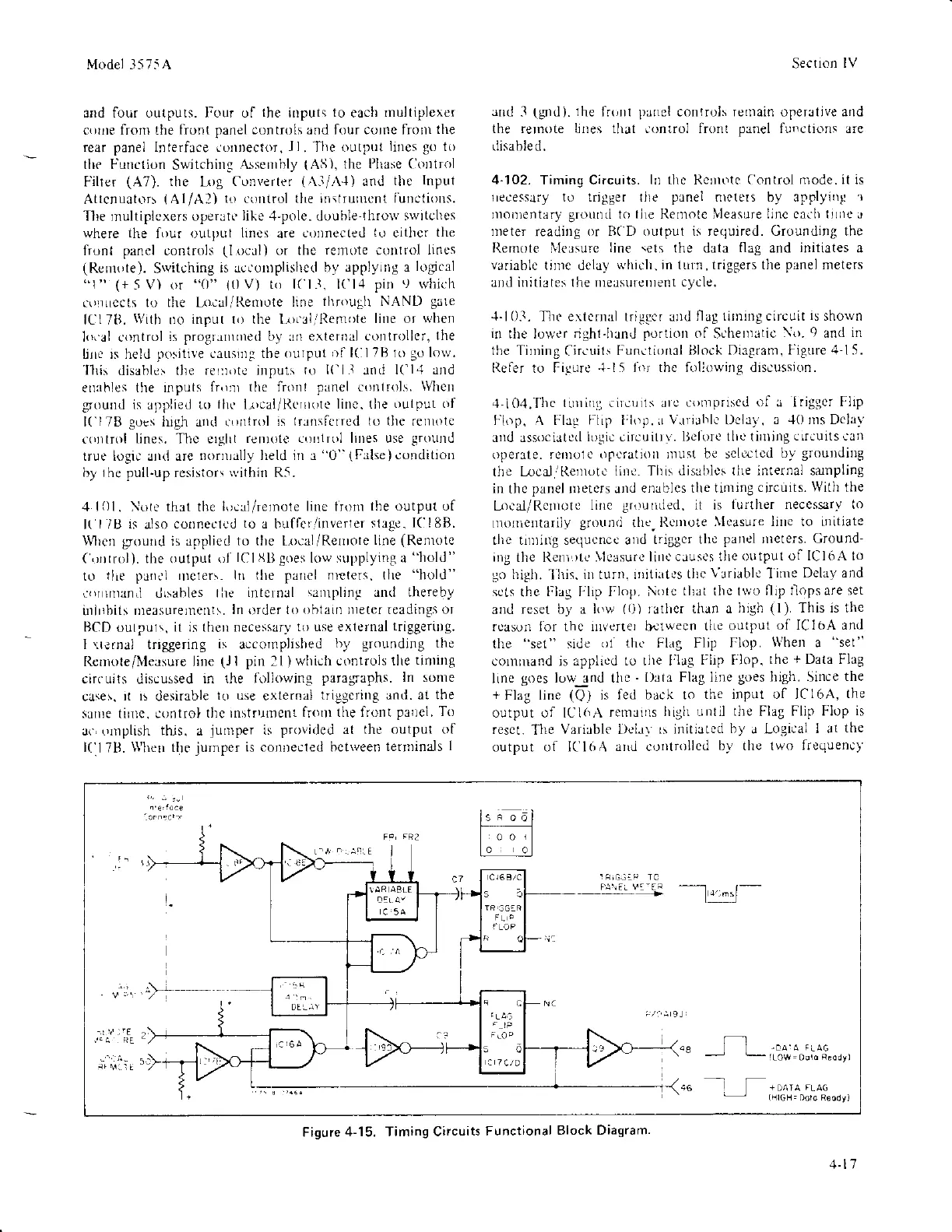
4-102.
Timing Circuits.
ln thc
Rernotc
Control nrode.it is
llecessaiy to lrisBer lile
panel
nreters by applyirtg
t
rnonlentary groilnd
to
llre
Ilemote
]! easure Iinc ca.h l,llrc J
rreter
reading
or B(D outpul is required. Grounding the
I{ernote
i\lr3sure
line
'ets
the date
flag
and
initiates
a
variablc
tirrc dclay
*hich. in tuln, triggers the
panel
meters
aDd initiates lhe nreasLlrerrenl cycle.
-1-10-1.
The e\lernal triggcr rnd
flag lirning circuit
is
shown
in
thr' Iower
rightJran,J
portion
of Schenrlic
\o.
9
and
in
the
'Tirning
Circuils
[:unrtional l]lock
Diagram. Figure 4-15.
llefer to fiiturc
-1-15
lr)r the foliorving discussion.
4-i04.lhc
1Lllli0!l .ircLrts ur0
.{)nrprLSed
of
l Iriggqr
Flip
frlop. A Fl.rg Flip t;lop. .r
V.u irhlc l)c1ri,
.
a
-10
lns Dclav
aI]d rssoci.ltc(l
iogic circ
u
itr
\. lJcli)rc llro tirtting
crr.uits can
operate. renrolc
()pcration
rnrlst be seloctcd
by"
grouliding
the Lr)cal/Relrrot.
linc. This
disablcs tlle inle(nal sarnpling
in
the
panel
ri)etcrs Jnd
enablcs the trnling
circuits.
With
the
Locai/Rerrotc
li,rc
gr(rLrlded. it is
lurther neccssary to
rnonrcntarily
grotrntl
lhc.
IlcDt,ute
Ilcasure ljtle to illitiate
the til ing sequcncc a
d trigB,cr thc
pancl
rnelers.
Cround-
illg
the lLerr,)tr
\lcasure lirtc
cliuscs tlle output
of IC l6A 1o
go higlr.
-l
his. i turn. i,ritiltcs
thq
Variablc
'1
ime Delay and
scLs
the
Flag I'lrp Irlop Note
that thc 1wo
ilip tloPsare set
and
reset
b)
a l(,w
(ll)
rallrcr than a
high (l). This is the
roason ibr thc utvcrter b,:twecn
tlLe output
of IC16A and
the
"set"
side
Lrl thr' fjl.rg Flip
Flop.
When
a
"sel"
cornnrand is
appliod Lo tlte lilag
FliP Flop.
the
+
Data Fla8
line
goes
lo$, and the
-
l)lta Flag line
goes
high. Since
the
+Flag
line
(O)
is
ied back to
the input of lCl6A,
the
output of ICI(rA
renrrins
higll until
lhe
Flag
Fllp ljlop
is
reset.
1l1e
Varirble Deh]
rs i,litiole.l
by
u Logical
I at
the
output oI I(ltrA
arrd cor]trolled
by the two
frequencl'
_-'.lt:l-
""
f l
-DA'a FLac
*
iLlw
-
0o!o
Reodr)
o"
-
f
*oara..ac
lBtcB:
Oolo R6ody)
Figure
4-15. Timing Circuits
Functional
Block Diagram.
1.11
 Loading...