Secrion
IV
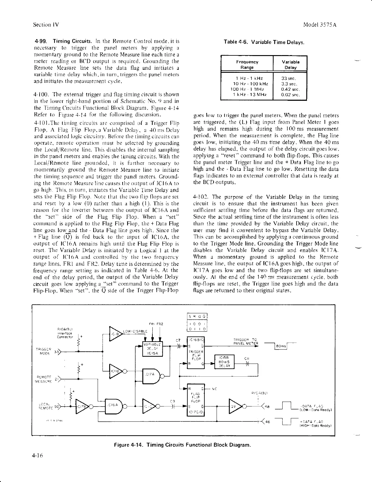
4-99. Timing Circuits.
In
lhe Renrote Con(rol mode. it is
Deuessary to trigger the
panel
nreters by
applying
a
nn)mentary
ground
to the Relnote l\leasure line each time
a
ineter
reading or
B('D
outpul is required. Crounding the
Rernotc N{casurc
line sets
the
data
flag and initi:rtes a
varieble time
deley
rvhich. in turn,lriggers the
panel
nreters
JoJ iIlilirle, llre
ll]e:r.urellrertl
.\.'l(.
4- i 00.
Tle exlernal trigger
and
flag liming circuit
is
shown
in
1he lower rightiand
portiol
o[ Schenlatic
No.
()
anC
in
the Tirning
Circuits
Functional Block Diagrum.
FigrrLe.l-1.1
Refer to
Figrrre4-l:1
for the iollowing
discussion.
"1-101.'the
tinirlg
circuits
arr'compriscd of a Trigger F'lip
Flop. A FIrg Flip Flop.
r Verirhlc
Dclar. a
.10
nrs Dch)
and associotcd logic circuitry.
Beii)re the tltling circuits cal
opcratg, rerDote operation
nlusr bc
sclect.d
by
grounding
the
l-ocal/ llenote line. This disables the
internal sanrpling
in the
panel
nreters
and
enables
the titning cirouits.
Witll
thc
l-ocal/Relnote line
!!rourded,
it is further necessary
to
nrollrelltarily
ground
the
ReI]rote lleasure line to itlitiate
the
til]ling secluence and triggcr the
pancl
mctcrs. Cround'
ing the Rcnlolc \'lcasure line.auses
the
output
of ICI6A to
go
high.
This. i tunl. iuitiatcs the Variable
f
irnc Delay
and
sets the Ftag FIip Flop. Note
that tlre two
flip llopsnre
set
and
reset
by a
low
(0)
ralhcr than e high (1).
This
is tlie
reason lirr
the
invcrter
betwecn the output of ICl(rA and
the
"sct"
side of the FIag
Flip I.lop.
\!'hen
a
"set"
cornrnand
is applied to the FIag Flip Fiop, thc
+
Data
Fiag
Iine
goes
lou'
and
the'Data
F-lag line
goes
high. Since the
+Flag
ljre
(Q)
k
ied
back to thc input of IC16A. the
output of lCl6A rernains high untrl
the Flag Flip Flop is
reset.
The Variable Delay is initiatsd
by a l.ogical I at
the
output of ICI6A ard colltrolled
b) lhe two
frcquency
range lines. FRI and FRl. Delal
tune is dctcrmined
by
the
frerluency
rarge settillg as intlicated
in Trble 4-6. At
the
end
of
the
delay
period, lhe oulput of
the Variable Delry
circuit
goes
low
applying
a
*sel"
command
to the
Trigger
Flip-Flop. \Vhen
"set".
the
Q
side of the lrigger
Flip-Flop
Ntodel 3575A
Table 4-6.
Variable
Time Delays.
Delav
1 Hz-1 kHz
1O Hz- 100 kHz
100
Hz I MHz
1 kHz
.
13 MHz
33 sec.
3.3 sec.
0.42
sec.
0.O2 sec.
goes
low
to
trigger the panel
meters.
\lhen
the
panel
meters
are triggered, the
(L)
Flag
input from Panel
l\,letcr
I goes
high artd remains high during the
l00ms
measuremen(
period.
When
the nreasurenrent
is
corrplete,
the
Flag line
goes
low,
initiating
the 40 ms time delay.
\\4ren the
40 rns
delay has elapsed. the output
of
the
delay circuit
goes
lo\\,.
applying
a
"reset"
comrnand
to
both flip-flops.'fhis causes
the
panel
meter Trigger
line
and the
+
Dala
Flag
line
to
go
high
and
the
-
Data FJag
line to go low.
Resetting the
data
flags indicates
1o an external cortroller that
data
is
ready at
the BCD
outputs.
.1-i0:.
The purpose
of
the
Variable Delay in the timing
circuit is to
elrsure that
the
instrument has
been
givel
sulficient
setlljng lime before the
data
flags are returned.
Since
the
actual
seltling time
of
the inslrument is
oflerr
less
than the time
provided
by the Variable Delay circuit. the
user
rray find i1
convenient 1rl
bypass
the Variable Delay.
This
can bc accompiished by applying
a
continuous
ground
to
(he
Trigger Mode line. Grounding the Trigger Nlode line
disables
the Variable Delay circuit and enables ICl7A.
\\4ren
a
momentary
ground is
applled
to
the Remote
Nleasure line, the
output of
ICI6A
goes
high.
lhe
oulput ol
I(ll7A goes
low
and
the two flip'flops are set simullane-
ously.
Al
the
end of
the l.ln
lns neasurenrent
(ycle.
both
flip-flops are reset, the Trigger line
goes
high and
the
data
flags are returled to their original states.
__lrryl-
,r,.
L r
r1
""
fl
lnra..-.
+
iLOw.
r
oro
R.od,
)
CE.]Y
c15
B
o"
-
f
-ro,o..r.
H
GF Doi.
peody)
4-16
Figure 4-14. Timing Circuits Functional Block Diagram.