B.5 Pin Assignments
The following table shows the Serial Adapter external connector pin
assignments.
+------------------------------------------------------------------------+
¦ Pin ¦ ¦ ¦ ¦
¦ No. ¦ ¦ ¦ ¦
¦ ¦ Signal Name¦ Directio¦ Description ¦
¦ ¦ ¦ ¦ ¦
+-----+------------+---------+-------------------------------------------¦
¦ 3 ¦ TX DATA ¦ Out ¦ Transmit Data ¦
+-----+------------+---------+-------------------------------------------¦
¦ 2 ¦ RX DATA ¦ In ¦ Receive Data ¦
+-----+------------+---------+-------------------------------------------¦
¦ 7 ¦ RTS ¦ Out ¦ Request to Send ¦
+-----+------------+---------+-------------------------------------------¦
¦ 8 ¦ CTS ¦ In ¦ Clear to Send ¦
+-----+------------+---------+-------------------------------------------¦
¦ 6 ¦ DSR ¦ In ¦ Data Set Ready ¦
+-----+------------+---------+-------------------------------------------¦
¦ 5 ¦ GND ¦ ¦ Signal Ground ¦
+-----+------------+---------+-------------------------------------------¦
¦ 1 ¦ DCD ¦ In ¦ Data Carrier Detect ¦
+-----+------------+---------+-------------------------------------------¦
¦ 4 ¦ DTR ¦ Out ¦ Data Terminal Ready ¦
+-----+------------+---------+-------------------------------------------¦
¦ 9 ¦ RI ¦ In ¦ Ring Indicator ¦
+------------------------------------------------------------------------+
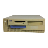
PS/2 Model L40 SX Quick Reference
Pin Assignments
¦ Copyright IBM Corp. 1991
B.5 - 1
 Loading...