22 POWER7 and POWER7+ Optimization and Tuning Guide
2.1 Introduction to the POWER7 processor
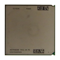
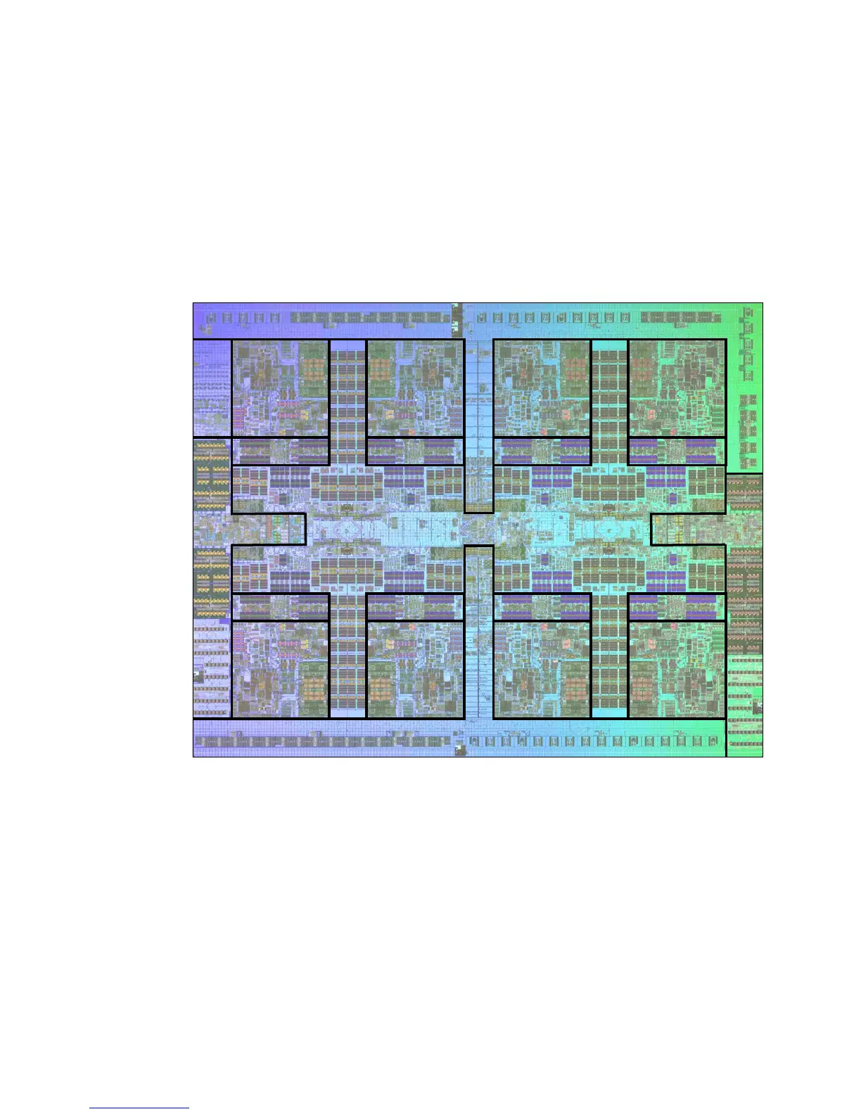
The POWER7 processor is manufactured using the IBM 45 nm Silicon-On-Insulator (SOI)
technology. Each chip is 567 mm
2
and contains 1.2 billion transistors. As shown in Figure 2-1,
the chip contains eight cores, each with its own 256 KB L2 and 4 MB L3 (embedded DRAM)
cache, two memory controllers, and an interconnection system that connects all components
within the chip. The interconnect also extends through module and board technology to other
POWER7 processors in addition to DDR3 memory and various I/O devices. The number of
memory controllers and cores available for use depends upon the particular POWER7
system.
Figure 2-1 The POWER7 processor chip
Each core is a 64-bit implementation of the IBM Power ISA (Version 2.06 Revision B), and
has the following features:
Multi-threaded design, capable of up to four-way SMT
32 KB, four-way set-associative L1 i-cache
32 KB, eight-way set-associative L1 d-cache
64-entry Effective to Real Address Translation (ERAT) for effective to real address
translation for instructions (2-way set associative)
64-entry ERAT for effective to real address translation for data (fully associative)
Aggressive branch prediction, using both local and global prediction tables with a selector
table to choose the best predictor
15-entry link stack
Core
L2 Cache
Core
L2 Cache
Core
L2 Cache
Core
L2 Cache
Core
L2 Cache
Core
L2 Cache
Core
L2 Cache
Core
L2 Cache
Mem Ctrl Mem Ctrl
L3 Cache and Chip Interconnect
Local SMP Links Remote SMP + I/O Links