Other Circuits
Speaker Circuit
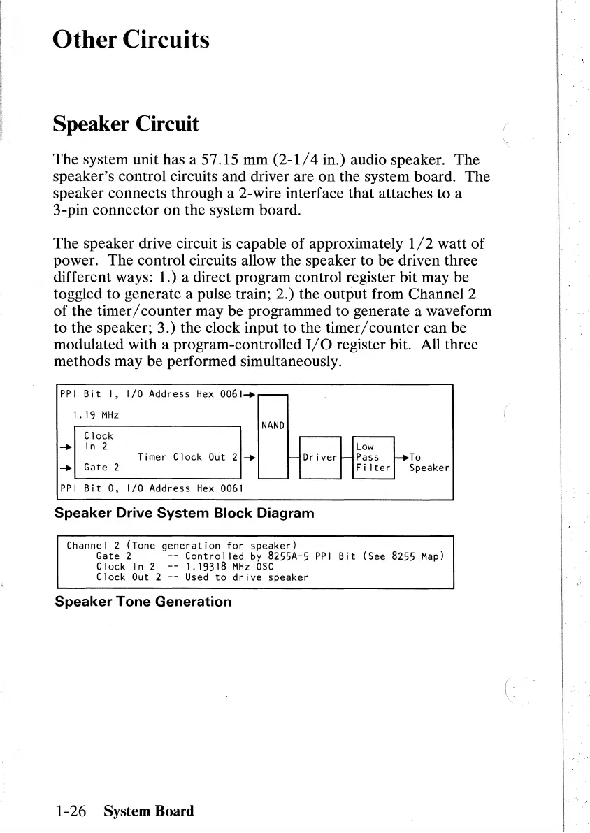
The system unit has a 57.15 mm
(2-1/4
in.) audio speaker. The
speaker's control circuits and driver are
on
the system board. The
speaker connects through a 2-wire interface that attaches to a
3-pin connector
on
the system board.
The speaker drive circuit
is
capable of approximately
1/2
watt of
power. The control circuits allow the speaker to be driven three
different ways: 1.) a direct program control register bit may be
toggled to generate a pulse train; 2.) the output from Channel 2
of
the
timer/counter
may be programmed to generate a waveform
to the speaker; 3.) the clock input to the
timer/counter
can be
modulated with a program-controlled
I/O
register bit. All three
methods may
be
performed simultaneously.
PPI
Bit
1,
I/O Address
Hex
0061-+
~
1.19
MHz
NAND
Clock
-+
In
2
Low
Timer Clock Out 2
-+
~
Driver
~
Pass
......
To
-+
Gate 2
Fi 1
ter
Speaker
-
PPI
Bit
0,
I/O Address
Hex
0061
Speaker
Drive System Block Diagram
Channel 2 (Tone
generation
for
speaker)
Gate 2
--
Controlled
by
8255A-5
PPI
Bit
(See 8255
Map)
Clock
In
2
--
1.19318
MHz
OSC
Clock Out 2
--
Used
to
drive
speaker
Speaker
Tone
Generation
1-26 System
Board