3-3
PLL CIRCUITS (MAIN UNIT)
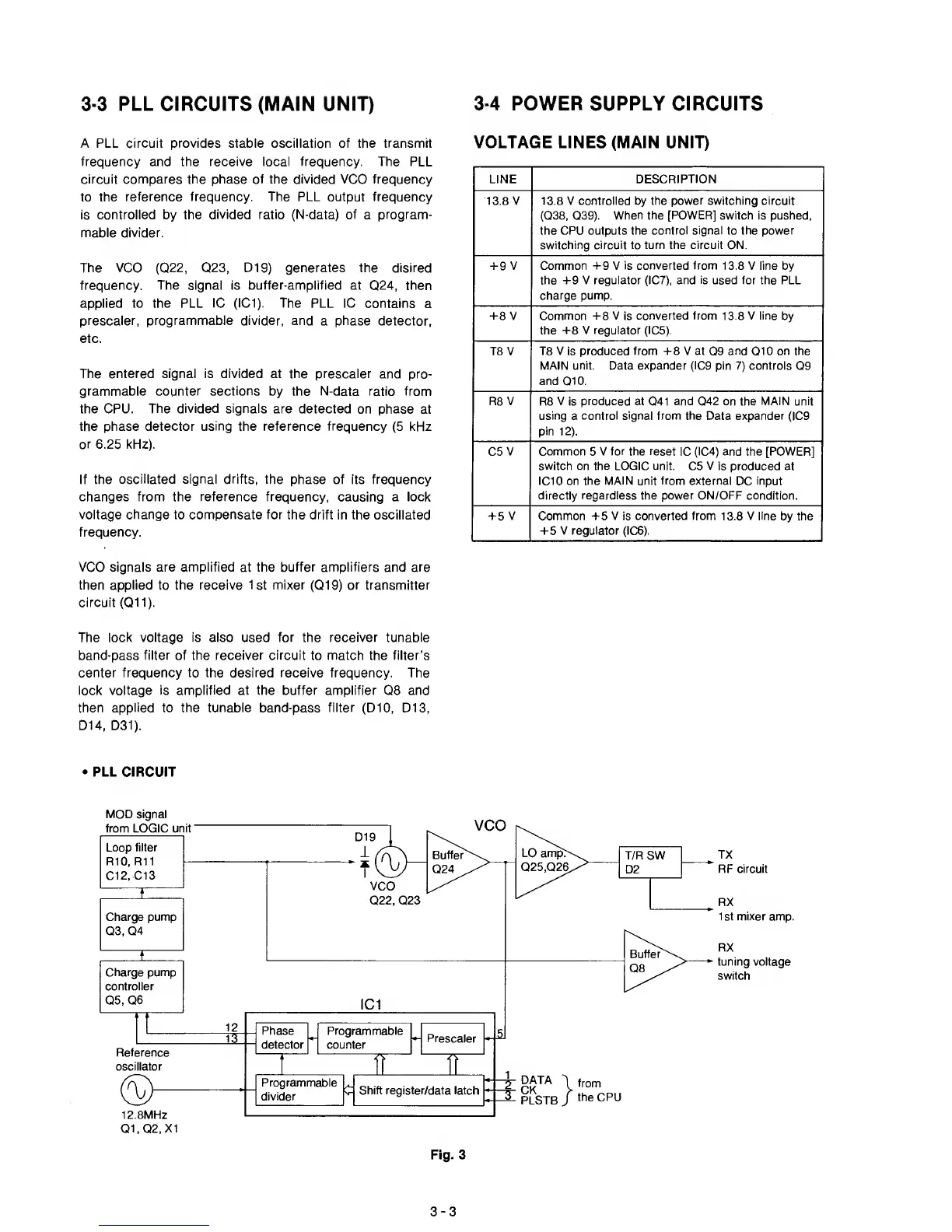
A PLL circuit provides stable oscillation of the
transmit
frequency and the receive local frequency. The PLL
circuit compares the phase of the divided VCO frequency
to the
reference frequency. The PLL output frequency
is controlled by the
divided ratio
(N-data)
of
a
program-
mable divider.
The VCO
(Q22,
Q23,
D19) generates the disired
frequency. The signal is buffer-amplified at
Q24,
then
applied to the PLL 1C
(IC1). The
PLL 1C contains
a
prescaler, programmable divider, and
a
phase
detector,
etc.
The entered signal Is divided at the prescaler
and pro-
grammable counter
sections
by the N-data ratio from
the CPU.
The divided signals are
detected on phase
at
the phase
detector using the reference frequency
(5
kHz
or 6.25 kHz).
If the
oscillated signal drifts,
the phase of its frequency
changes
from the reference frequency,
causing a lock
voltage change
to
compensate for
the drift In the oscillated
frequency.
VCO signals are amplified at the buffer amplifiers and are
then applied
to
the receive
1st
mixer
(019)
or transmitter
circuit (Oil).
3-4
POWER SUPPLY CIRCUITS
VOLTAGE LINES (MAIN UNIT)
LINE
DESCRIPTION
13.8 V 13.8 V controlled by the
power
switching circuit
(Q38,
Q39).
When the [POWER]
switch is pushed,
the CPU outputs the
control signal
to
the power
switching circuit to turn the circuit ON.
-1-9
V Common
-1-9
V
is converted from
13.8 V line by
the
-1-9
V regulator (IC7), and
is
used for the PLL
charge pump.
-i-e
V
Common -t-8 V is converted from 13.8 V line
by
the
-1-8
V regulator (ICS).
T8 V
T8 V is produced from
-1-8
V at
09
and
01 0
on the
MAIN
unit.
Data
expander (IC9
pin
7)
controls
09
and 01
0.
R8 V R8 V is produced at 041 and 042 on the MAIN unit
using
a
control signal from the
Data
expander
(IC9
pin
12).
C5 V
Common
5 V
for
the
reset
1C
(IC4)
and the [POWER]
switch on the LOGIC unit. C5 V is produced
at
IC10 on the MAIN unit from external
DC input
directly
regardless
the
power
ON/OFF condition.
-1-5
V Common
-1-5
V
is
converted from 13.8 V
line by
the
-1-5
V
regulator (IC6).
The
lock voltage is also
used
for the receiver tunable
band-pass
filter of the receiver circuit
to
match
the
filter’s
center frequency to the desired receive frequency. The
lock voltage is
amplified
at the buffer amplifier 08 and
then
applied
to
the tunable band-pass filter (DIO,
D13,
D14, D31).
•
PLL CIRCUIT
TX
RF circuit
RX
1 St mixer amp.
RX
tuning voltage
switch
Fig. 3
3-3