SECTION
3 CIRCUIT
DESCRIPTION
3-1
VHF RECEIVER
CIRCUITS
3-1-1
ANTENNA SWITCHING
CIRCUIT
(HPF UNIT)
The received signals that
pass through
the LPF
UNIT are
separated as VHF and
UHF signals on
the HPF UNIT
and are
applied to each RF
amplifier circuit.
The HPF UNIT contains
a high-pass
filter, low-pass
filter and
an antenna switching circuit.
The VHF
signals pass
through
the low-pass filter
(L3-L5, C6~C10)
and the antenna
switching
circuit (C12~C14,
L6, L7, D2). The
VHF signals
and are then
applied to the V*RF
UNIT. The high-pass
filter
(C1~C5, LI, L2) is designed
for UHF receiving
and does
not
allow VHF signal passage.
3-1-2
RF AND 1ST MIXER
CIRCUITS
(V.RF
UNIT)
The
RF
and 1st mixer circuits
are located on
the V»RF UNIT
where the signals are amplified at Q1
and Q2 and are then
converted
to a 1st
IF signal
at Q3. The frequency
of the
1st
IF signal is 30.875 MHz.
Q3
converts the
RF signal using the
V*PLL output signal
coming from the "LLO” line.
The VHF RF circuit adopts a tuned bandpass
filter circuit
that
tunes the filters
to
the
center
frequency
of the
receiving
signal using varactor
diodes (D2, D4, D5).
A PLL lock
voltage is used for the filter tuned signal.
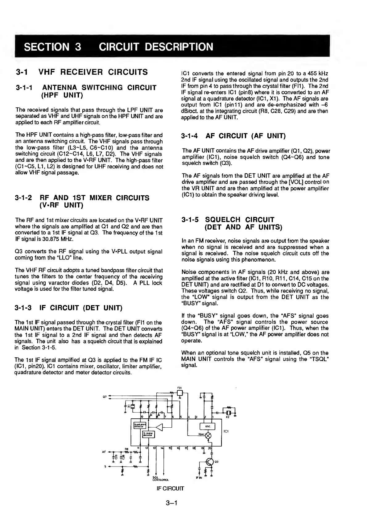
3-1-3
IF CIRCUIT (DET
UNIT)
The 1st IF signal passed through the crystal
filter (F11
on the
MAIN UNIT) enters the
DET UNIT. The DET UNIT
converts
the 1st IF signal to a 2nd IF signal and then
detects AF
signals.
The
unit also
has a squelch circuit that
is explained
in Section
3-1 -5.
The
1 St IF
signal amplified
at Q3 is
applied to the FM IF
1C
(IC1
,
pin20).
IC1 contains mixer, oscillator,
limiter amplifier,
quadrature
detector and meter
detector circuits.
IC1 converts
the
entered signal from
pin 20
to a 455 kHz
2nd IF
signal
using the
oscillated signal
and outputs the 2nd
IF from
pin 4 to
pass
through the
crystal filter
(FI1 ). The 2nd
IF signal re-enters IC1 (pin8) where it is converted to an AF
signal
at a
quadrature detector (IC1
,
XI ).
The AF signals
are
output from IC1 (pinll) and are de-emphasized with
-6
dB/oct.
at the
integrating circuit (R8,
C28, C29)
and are then
applied
to the
AF UNIT.
3-1-4
AF CIRCUIT (AF UNIT)
The AF UNIT contains
the AF drive amplifier
(Q1
, Q2),
power
amplifier (IC1), noise squelch switch
(Q4~Q6)
and tone
squelch switch
(Q3).
The
AF signals from the DET UNIT are
amplified at the AF
drive
amplifier and are passed through the
[VOL] control
on
the
VR UNIT and are then amplified at the power amplifier
(IC1) to obtain the speaker driving level.
3-1-5
SQUELCH
CIRCUIT
(DET AND AF
UNITS)
In
an FM receiver, noise signals are output from
the
speaker
when no signal is
received
and are suppressed when a
signal is received. The
noise
squelch
circuit cuts off the
noise signals using this phenomenon.
Noise components in AF signals
(20
kHz
and above) are
amplified at the active filter (IC1, RIO, R11,
Cl
4,
C15 on the
DET UNIT) and are rectified
at D1
to convert
to DC voltages.
These voltages
switch
Q2. Thus,
while
receiving no signal,
the "LOW” signal is output from the DET
UNIT as the
“BUSY”
signal.
If the "BUSY” signal goes down, the “AFS” signal
goes
down. The “AFS” signal controls the power
source
(Q4-Q6)
of the AF power amplifier (IC1).
Thus, when the
"BUSY”
signal is at “LOW,” the AF power
amplifier does not
operate.
When an
optional tone squelch unit is installed,
05 on the
MAIN UNIT
controls the “AFS” signal
using the
“TSQL”
signal.
Fll
IF
CIRCUIT
3-1