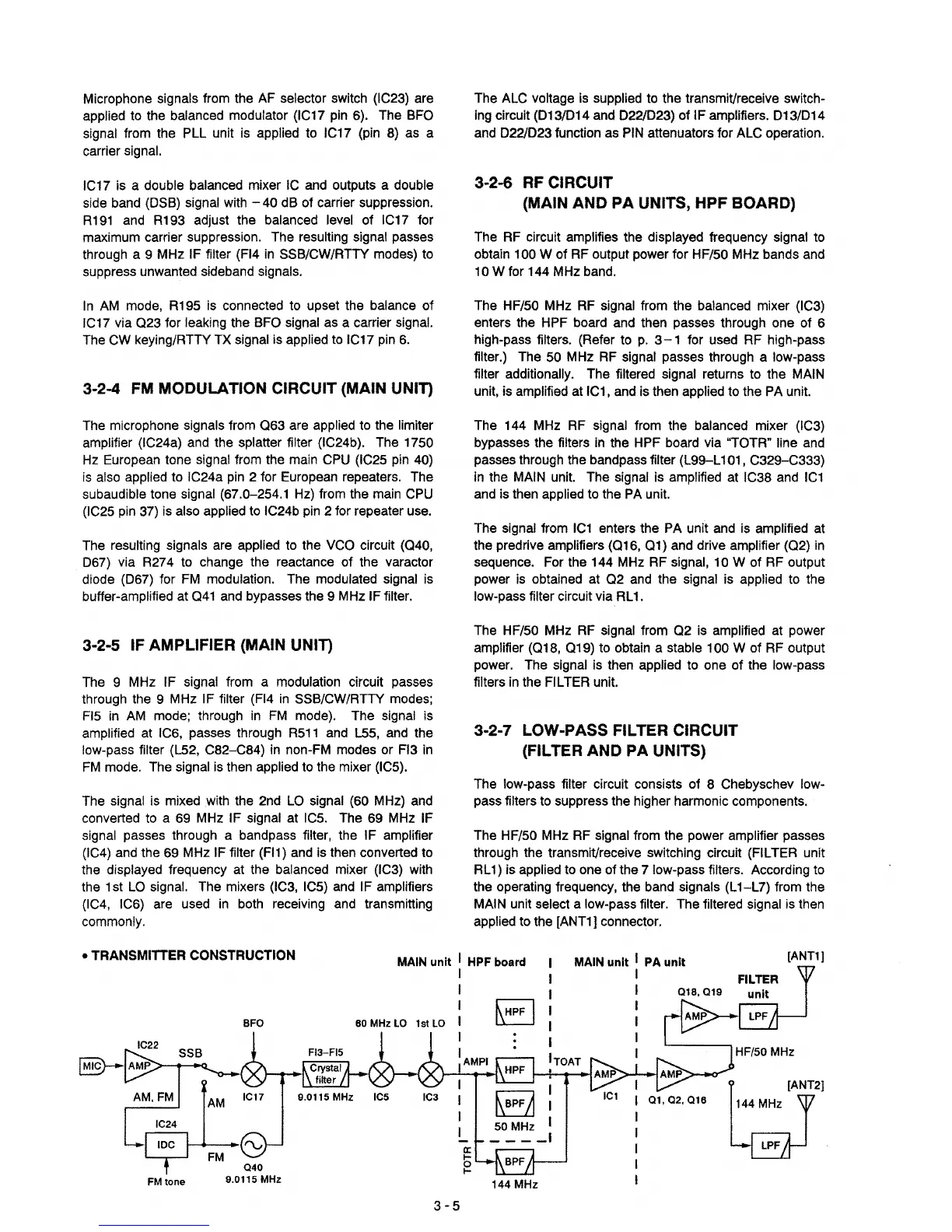
Microphone signals from the
AF
selector switch (IC23) are
applied
to
the balanced modulator (IC17
pin
6).
The
BFO
signal from the
PLL
unit is applied to IC17 (pin
8)
as
a
carrier signal.
IC17 is a double balanced mixer
IC
and outputs a double
side band
(OSB)
signal with
-40
dB of carrier suppression.
R191
and
R193 adjust the balanced level of
IC17
for
maximum carrier suppression. The resulting signal passes
through a 9 MHz IF filter
(F14
in
SSB/CW/RTTY modes)
to
suppress unwanted sideband signals.
In
AM
mode, R195
is
connected
to
upset the balance of
IC17 via
023
for leaking the
BFO
signal
as
a carrier signal.
The
CW
keying/RTTY
TX
signal is applied
to
IC17
pin
6.
3-2-4
FM
MODULATION CIRCUIT (MAIN UNIT)
The microphone signals from
063
are applied
to
the limiter
amplifier (IC24a)
and
the splatter filter (IC24b). The 1750
Hz
European tone signal from the main
CPU
(IC25
pin
40)
is
also applied to IC24a
pin
2 for European repeaters. The
subaudible tone signal (67.0-254.1
Hz)
from the
main
CPU
(IC25
pin
37) is also applied to IC24b
pin
2 for repeater use.
The resulting signals are applied to the
VCO
circuit (040,
067) via
R274
to
change the reactance of the varactor
diode (067) for
FM
modulation. The modulated signal is
bUffer-amplified at 041
and
bypasses the 9 M
Hz
IF filter.
3-2-5 IF AMPLIFIER (MAIN UNIT)
The 9
MHz
IF signal from a modulation circuit passes
through the 9
MHz
IF filter
(F14
in
SSB/CW/RTTY modes;
FI5
in
AM
mode; through
in
FM
mode). The signal is
amplified at
IC6,
passes through
R511
and
L55,
and
the
low-pass filter (L52, C82-C84)
in
non-FM modes or FI3 in
FM
mode. The signal
is
then applied
to
the mixer (IC5).
The signal
is
mixed with the
2nd
LO
signal (60
MHz)
and
converted
to
a
69
MHz
IF signal at
IC5.
The 69
MHz
IF
signal passes through a bandpass filter, the IF amplifier
(IC4) and the 69
MHz
IF filter
(Fll)
and
is then converted to
the displayed frequency at the balanced mixer (IC3) with
the 1st
LO
signal. The mixers
(IC3,
IC5)
and
IF amplifiers
(IC4,
IC6) are used
in
both
receiving
and
transmitting
commonly.
The
ALC
voltage
is
supplied
to
the transmiVreceive switch-
ing circuit (013/014 and 022/023) of IF amplifiers. 013/014
and
022/023 function
as
PIN
attenuators for ALC operation.
3-2-6
RF
CIRCUIT
(MAIN AND PA UNITS, HPF BOARD)
The
RF
circuit amplifies the displayed frequency signal
to
obtain 100 W of
RF
output power for HF/50 MHz bands and
10 W for 144 MHz band.
The HF/50
MHz
RF
signal from the balanced mixer (IC3)
enters the HPF board and then passes through one of 6
high-pass filters. (Refer to
p.
3-1
for used RF high-pass
filter.) The
50
MHz
RF
signal passes through a low-pass
filter additionally. The filtered signal returns to the
MAIN
unit, is amplified at IC1, and is then applied to the
PA
unit.
The 144
MHz
RF
signal from the balanced mixer (IC3)
bypasses the filters
in
the HPF board via "TOTR" line
and
passes through the bandpass filter (L99-L
101
, C329-C333)
in
the
MAIN
unit. The signal is amplified at IC38
and
ICl
and
is then applied to the
PA
unit.
The signal from
ICl
enters the
PA
unit
and
is amplified at
the predrive amplifiers (016,
01)
and drive amplifier (02) in
sequence. For the 144
MHz
RF
signal, 10 W of
RF
output
power
is
obtained at
02
and
the signal is applied to the
low-pass filter circuit via RL
1.
The HF/50
MHz
RF
signal from
02
is
amplified
at
power
amplifier (018. 019)
to
obtain a stable 100 W of
RF
output
power. The signal is then applied to one of the low-pass
filters
in
the FILTER unit.
3-2-7 LOW-PASS FILTER CIRCUIT
(FILTER AND PA UNITS)
The low-pass filter circuit consists of 8 Chebyschev low-
pass filters to suppress the higher harmonic components.
The HF/50
MHz
RF
signal from the power amplifier passes
through the transmiVreceive switching circuit (FILTER unit
RL
1)
is applied to one ofthe 7 low-pass filters. According to
the operating frequency, the band signals (L1-L7) from the
MAIN
unit select a low-pass filter. The filtered signal
is
then
applied to the [ANT1] connector.
• TRANSMITTER CONSTRUCTION
9.0115 MHz IC5
IC3
3-5
144 MHz
MAIN unit I PA unit
I
I
018.
019
I
I
I
I
01. 02.
016
[ANT1]
FILTER
unit
[ANT2]
144 MHz
 Loading...