012
through
033
are matrix diodes
to
convert the band
signal into hexadecimal
code
for
the
CPU.
The
output
signal from
the
mixer
is
then fed
to
the
BPF
unit. The
BPF
unit
is
composed
of
a high-pass filter, low-
pass filter and band-pass filter for each band, and buffer
amplifiers.
The high-pass filter
is
composed
of
C1
through C5, and
L1
and L2.
The low-pass filter
is
composed
of
C6 through C13 and
L3
through L5.
The band-pass filters are provided for each band and
selected one of them by
the
band signal from
the
band
switch.
The signal passed through
the
high-pass filter, low-pass
filter and a band-pass filter
is
then fed
to
the
buffer am-
plifiers,
01,
02
and
03.
The
output
of
03
is
then fed
to
the
mixer consisting
of
04
through
07
in
the
RF unit as
the
1st local oscillator signal.
3.
LOGIC CIRCUITS
The logic circuits control operating frequency, band, mode,
PLL, display etc., and are designed for low power con-
sumption and high speed operation using a CMOS 4-bit
CPU.
The
CPU,
IC1
is
a plastic package with
42
pins.
CLO
and
CL 1
of
pins 1 and
42
are
the
clock terminals for this CPU,
oscillating
at
about
400kHz with
X1
ceramic oscillation
unit.
The
CPU
has a total
of
9
input
and
output
ports, each
sharing its own function:
Port A - 4 bit
input
Decodes
the
port
E
output
as shown
in
the matrix table
to
expand input functions with time sharing.
Port B - 4
bit
input
Used as an input
port
for
the
sensor (tuning control).
Port C - 4 bit
output
Outputs
the
2nd
local oscillator 100Hz steps
0/
A convert-
ing signal.
Port 0 - 4 bit
output
Outputs
the
2nd
local oscillator 10Hz steps O/A converting
signal.
Port E - 4
bit
output
Outputs
various
data
as a general purpose
output
terminals.
Port F - 3 bit
output
FO
; Strobe signal
output
for display.
F 1 : Load signal
output
for PLL above 1 kHz digit.
F2 : Reset signal
output
for display.
Ports G and H are
not
used.
3-7
Port
I - 1 bit
output
10
: Reset signal
output
for sensor counter.
When
the
power switch
is
turned on, 13.
av
DC
is
applied
to
IC9, voltage regulator, through R2 and
01.
ICg
puts
out
regulated 5V.
At
the
same time,
02
is
turned on and
supplies
the
regulated
5V
as
the
power source of
the
LOGIC unit. When a memory backup power source
is
con-
nected,
the
power
is
applied
to
ICg through R1, and
re-
gulated 5V
is
supplied
to
IC1,
the
CPU
to
maintain
the
operating frequency, memorized frequency, etc.
At
this
time,
02
is
turned
off
and 5V
is
not
supplied for
the
other
circuits.
At
the
moment
of
the
power switch has been
turned
on,
a pulse
is
fecfto
pin 3
of
Ica
through C3. After
the
pulse
has been waveform-shaped, it
is
fed
to
the
reset terminal
(pin 7)
of
IC1,
to
initialize
the
CPU.
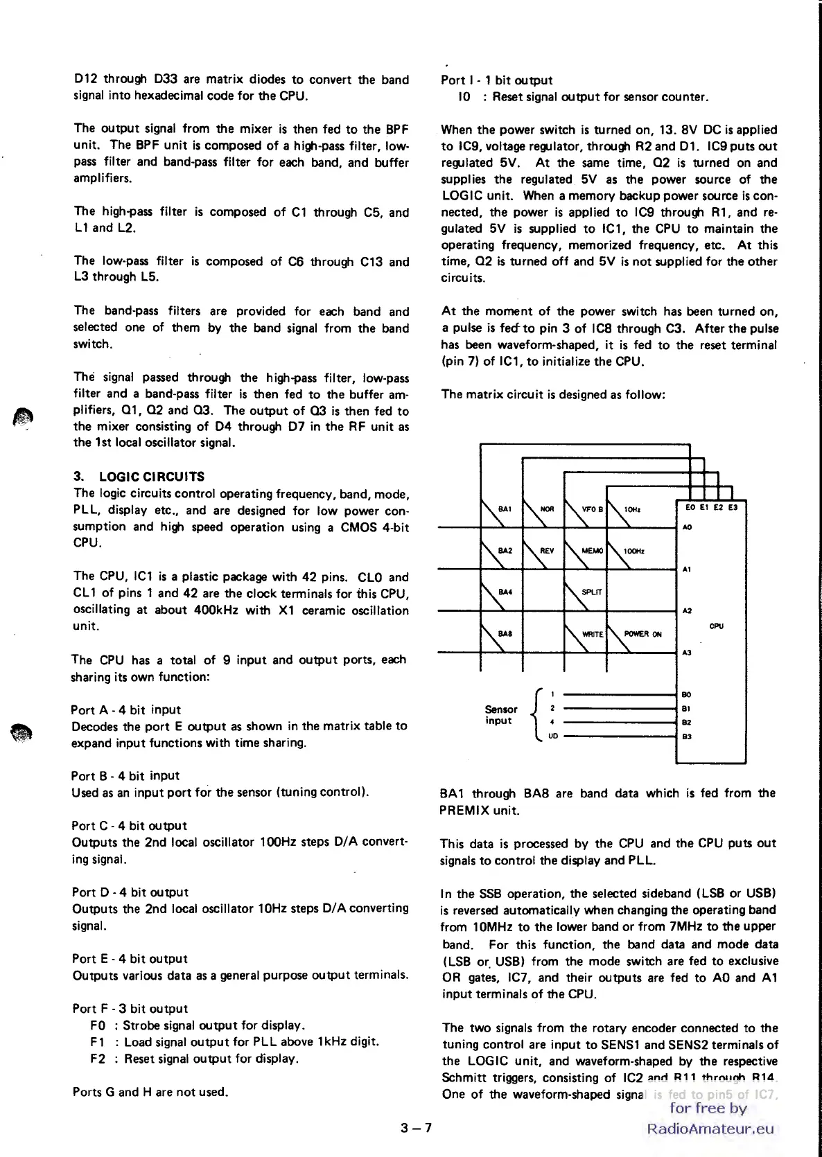
The matrix circuit
is
designed as follow:
I
I I
",1
~NOR
I'\0B
I'\OHZ
EO
El
E2 E3
AO
",2
~EV
~E~
~z
Al
~4
~sPLIT
A2
1'\8
~WRITE
~~ON
CPU
1.3
L
eo
Sensor
Bl
input
B2
B3
BA
1 through BAa are band data which
is
fed from the
PREMIX unit.
This data
is
processed by
the
CPU
and
the
CPU
puts
out
signals
to
control
the
display and PLL.
In
the
SSB
operation,
the
selected sideband (LSB
or
USB)
is
reversed automatically when changing
the
operating band
from 10MHz
to
the
lower band
or
from 7MHz
to
the
upper
band. For this function, the band data and
mode
data
(LSB or. USB) from
the
mode
switch are fed
to
exclusive
OR gates, IC7, and their
outputs
are fed
to
AO
and A 1
input terminals
of
the
CPU.
The two signals from
the
rotary encoder connected
to
the
tuning control are input
to
SENS1 and SENS2 terminals
of
the
LOGIC unit, and waveform-shaped by
the
respective
Schmitt triggers, consisting
of
IC2 and
R11
through R14.
One
of
the
waveform-shaped signal
is
fed
to
pin5 of IC7.
for
free
by
RadioAmateur.eu
 Loading...