4 - 4
4-5 PORT ALLOCATIONS
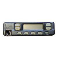
• CPU (MAIN-A/B/C UNIT: IC35)
Pin
No.
Port
Name
Description I/O
A3 NWC1
Bandwidth switches (Q27–Q29, D8, D16)
control.
“High”=While operating in the wide mode.
O
B3 DUSE CTCSS/DTCS switch (Q12) control. O
B11 CENC0 CTCSS/DTCS tone encode signals. O
B12 NOIS Noise signal from the IF IC (IC15). I
B13 DDST
Strobe signal to the DTMF decode IC (MAIN-A/
B/C UNIT: IC10).
O
C6 ESCL Serial clock to the EEPROM (IC36). O
C8 FSDA
Serial data to the expander (FRONT UNIT:
IC702 and IC703).
O
C11 CENC1 CTCSS/DTCS tone encode signals. O
C12 POSW
Power switch (VR UNIT: R502).
“Low”=While the power is ON.
I
C13 MTCK
Serial clock to the baseband IC (MAIN-A/B/C
UNIT: IC4).
O
C14 DDSD Serial data to the DTMF decode IC (IC10). O
D4 NWC2
Bandwidth switches (Q18, D3, D4) control.
“High”= While operating in the narrow or digital
mode.
O
D6 ESDA Serial data to the EEPROM (IC36). I/O
D8 FSCL
Serial clock to the expanders (FRONT UNIT:
IC702 and IC703).
O
D11 CENC2 CTCSS/DTCS tone encode signals. O
D12 DDAC Serial clock to the DTMF decode IC (IC10). O
D13 MSCK
Serial clock to the baseband IC (MAIN-A/B/C
UNIT: IC4).
O
D15 CSFT
CPU clock frequency shift control.
“High”=The clock frequency is shifted.
O
E13 RES
CPU reset signal from the reset IC (IC34).
“High”=CPU is reset.
I
K1–
K3
CBI0−2 [ROTARY SELECTOR] (VR UNIT: S501). I
L1 EMER [Emer] (VR UNIT: S501). I
L2 SIDE1
[Side1] (S3).
“Low”=Pushed.
I
L3 CBI3 [ROTARY SELECTOR] (VR UNIT: S501). I
L4 SIDE2
[Side2] (S2).
“Low”=Pushed.
I
M1 SIDE3
[Side3] (S1).
“Low”=Pushed.
I
M3 TLED
TX indicator (FRONT UNIT: DS710) control.
“High”=While transmitting.
O
M4 S5C
S5V line control.
“Low”=While in the power save mode.
O
M5 PMFM PM/FM switch (IC13) control. O
M7 RMUTO
AF mute switch (IC8) control.
“Low”=Mute.
O
M8 SENC Single tone encode signal. O
M11 BATV Battery voltage. I
M14 IPTT
[PTT] (S4).
“Low”=Pushed.
I
N1 RLED
RX indicator (FRONT UNIT: DS710) control.
“High”=While receiving a signal.
O
N2 UNLK
PLL IC (IC14) unlock detect.
“Low”=Unlocked.
I
N4 PWON
VCC line control.
“Low”=While the power is ON.
O
N5 T5C
T5V line control .
“Low”= While transmitting.
O
N8 BEEP Beep sound (Square wave). O
N10 SDEC Decoded 2/5 tone and DTMF signals. I
N12 RSSI RSSI voltage from the IF IC (IC15). I
P1 SCK
Serial clock to the PLL IC (IC14) and D/A
converter (IC9).
O
Pin
No.
Port
Name
Description I/O
P2 SSO
Serial data to the PLL IC (IC14) and D/A
converter (IC9).
O
P3 DAST Strobe signal to the D/A converter (IC9). O
P4 DASW
Outputs mode (Digital/Analog) switching
control.
“High”=While operating in the analog mode.
O
P5 R5C
R5V line control.
“Low”= While receiving.
O
P6 EMPH
Outputs emphasis characteristic switching
control.
O
P12 LVIN Lock voltage. I
R1 TMUT
Transmit mute switch (RF UNIT: Q604) control.
“High”=Mute.
O
R2 DSDA Serial data to the D/A converter (IC33). O
R4 PLST PLL strobe signal to the PLL IC (IC14). O
R3 MTDT
Serial data to the baseband IC (MAIN-A/B/C
UNIT: IC4).
O
R10 CDEC CTCSS/DTCS signals. I
Pin
No.
Port
Name
Description
1T1
Tuning voltage to the tuned BPF (
D21,D24, L27,
L29, C308, C309, C320, C322, C323,
).
2T2
• While receiving
Tuning voltage to the tuned BPF (
D17, D18,
L23, L25, C273, C278, C287, C291
).
• While transmitting
TX power setting voltage to the APC AMP (RF
UNIT: IC601).
3TLVA
Oscillating frequency adjustment voltage to the TX
VCO (Q32, D9, D12, D13).
4RLVA
Outputs oscillating frequency adjust voltage to the
RX VCO-A/B (
Q30, D10, D14/Q31, D11, D15).
Pin
No.
Port
Name
Description
4 AFON
AF power amplifi er (IC705 and IC706) control.
“High”=Activated.
5 LIGH
LCD backlight control.
“High”=While the backlight lights.
6 SPCON
Internal or external speaker select.
“Low”=While the internal speaker is used.
7 MCON
Internal or external microphone select.
“Low”=While the internal microphone is used.
• D/A CONVERTER (MAIN-A/B/C UNIT: IC33)
• EXPAND IC (FRONT UNIT: IC702)
 Loading...