IC BLOCK DIAGRAMS AND TERMINAL DESCRIPTIONS -33
TERMINAL DESCRIPTION
U8031: S29GL128N (128 Mbit Flash Memory)
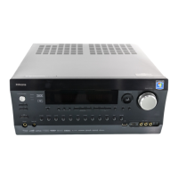
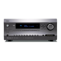
TX-SR876/SA876
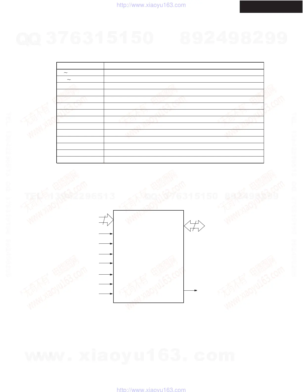
LOGIC SYMBOL
DQ0 ~ DQ15
(A-1)
RY/BY#
BYTE#
V
IO
OE#
CE#
A0 ~ A22
WE#
23
16 or 8
WP#/ACC
RESET#
A0 A22
DQ0 DQ14
DQ15 / A-1
DQ15(Data Input/Output: Word Mode), A-1(LSB Adress Input: Bite Mode)
BYTE#
CE#
OE#
WE#
RESET#
WP# / ACC
RY / BY#
Ready / Busy Output
V
CC
V
IO
V
SS
NC
Adress Input(23 pins)
Data Input/Output(15 pins)
Selector of 8 bit Mode and 16 bit Mode
Chip Enable
Output Enable
Write Enable
Hardware Reset Pin
Hardware Write Protect Input/Acceleration Input
3.0V Power Supply
Output Buffer Power Supply
GND
No Connection
PIN DESCRIPTION
w
w
w
.
x
i
a
o
y
u
1
6
3
.
c
o
m
Q
Q
3
7
6
3
1
5
1
5
0
9
9
2
8
9
4
2
9
8
T
E
L
1
3
9
4
2
2
9
6
5
1
3
9
9
2
8
9
4
2
9
8
0
5
1
5
1
3
6
7
3
Q
Q
TEL 13942296513 QQ 376315150 892498299
TEL 13942296513 QQ 376315150 892498299
http://www.xiaoyu163.com
http://www.xiaoyu163.com
 Loading...