Technical Reference
49
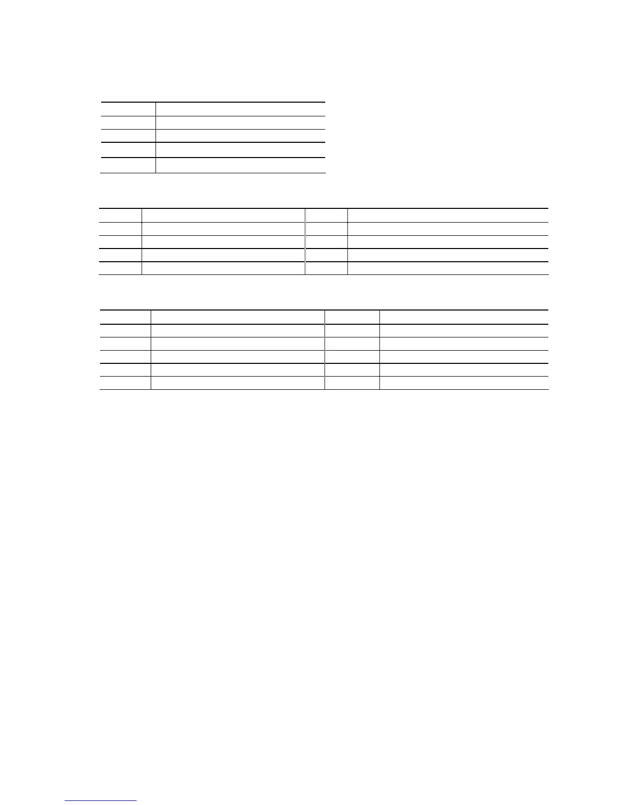
Table 18. Processor (4-Pin) Fan Header
Pin Signal Name
1 Ground
2 +12 V
3 FAN_TACH
4 FAN_CONTROL
Table 19. Front and Rear Chassis Fan Headers
Pin 4-Wire Support Pin 3-Wire Support
1 Ground 3 Ground
2 +12 V 2 FAN_POWER
3 FAN_TACH 1 FAN_TACH
4 FAN_CONTROL N/A N/A
Table 20. Front Panel IEEE 1394a Header
Pin Signal Name Pin Signal Name
1 Data A (positive) 2 Data A (negative)
3 Ground 4 Ground
5 Data B (positive) 6 Data B (negative)
7 +12V_DC 8 +12 V_DC
9 Key (no pin) 10 Ground
Note: The +12 V DC power on the IEEE 1394a header is fused.
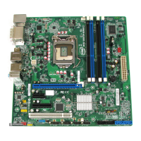
2.2.2.2 Add-in Card Connectors
The board has the following add-in card connectors:
• One PCI Express 2.0 x16: this connector supports simultaneous transfer speeds of
up to 8 GB/s of peak bandwidth per direction.
• PCI Express 2.0 x4: one PCI Express 2.0 x4 connector. The x4 interface supports
simultaneous transfer speeds up to 500 MB/s of peak bandwidth per direction and
up to 4 GB/s concurrent bandwidth.
• PCI Express 2.0 x1: one PCI Express 2.0 x1 connector. The x1 interface supports
simultaneous transfer speeds up to 1 GB/s of peak bandwidth per direction and up
to 2 GB/s concurrent bandwidth.
• One Conventional PCI (rev 2.3 compliant) connector.
Note the following considerations for the Conventional PCI bus connector:
• The Conventional PCI bus connector is bus master capable.
• SMBus signals are routed to the Conventional PCI bus connector. This enables
Conventional PCI bus add-in boards with SMBus support to access sensor data on
the desktop board. The specific SMBus signals are as follows:
⎯ The SMBus clock line is connected to pin A40.
⎯ The SMBus data line is connected to pin A41.