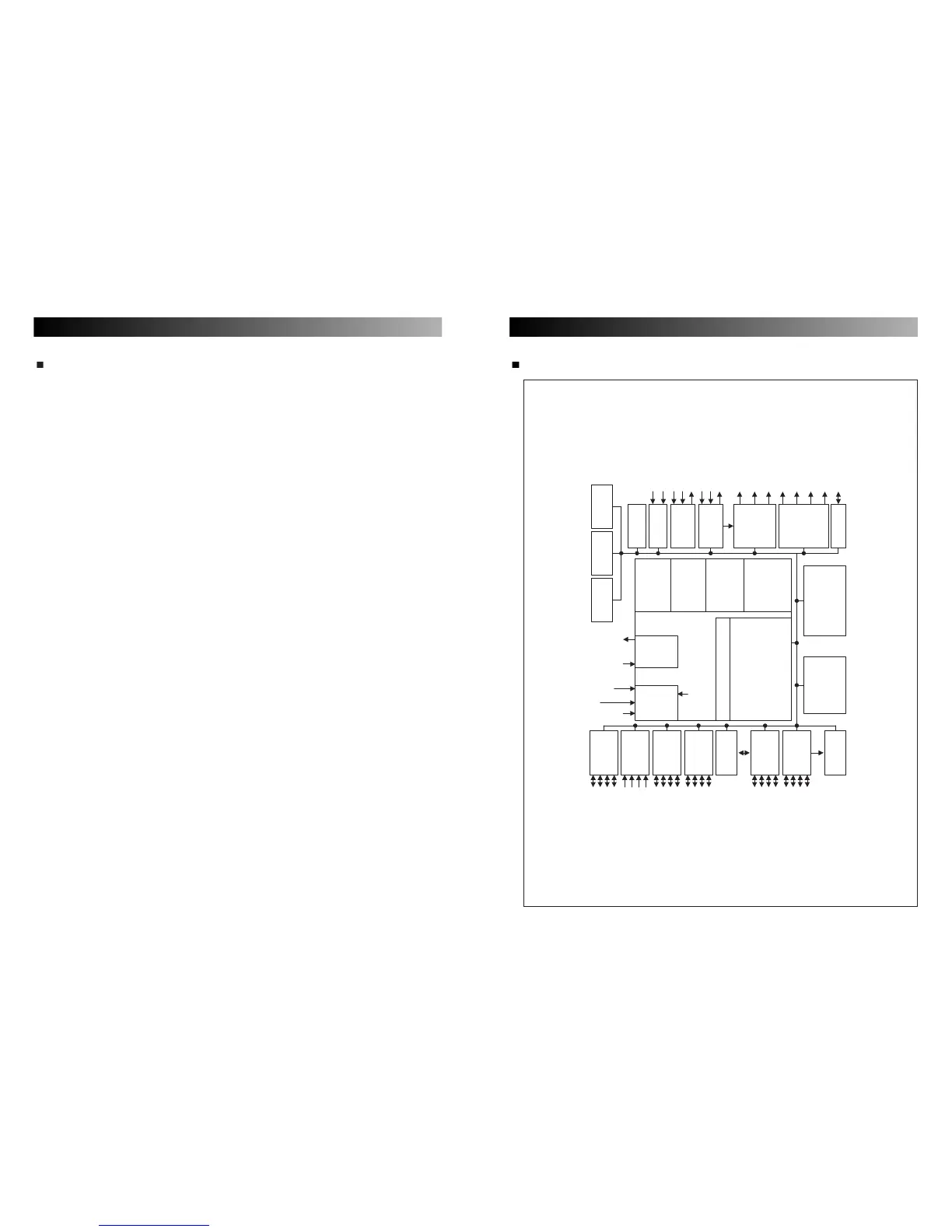
FEATURES
Memory
• 512-nibble RAM
• 16K-byte ROM
I/O Pins
• Input only: 4 pins
• Output only: 28 pins
• I/O: 24 pins
LCD Controller/Driver
• Maximum 14-digit LCD direct drive capability
• 28 segment x 4 common signals
• Display modes: Static, 1/2 duty (1/2 bias)
1/3 duty (1/2 or 1/3 bias), 1/4 duty (1/3 bias)
8-Bit Basic Timer
• Programmable interval timer functions
• Watch-dog timer function
8-Bit Timer/Counter
• Programmable 8-bit timer
• External event counter
• Arbitrary clock frequency output
• External clock signal divider
• Serial I/O interface clock generator
Watch Timer
• Time interval generation
: 0.5 s, 3.9 ms at 32.768 kHz
• Frequency outputs to BUZ pin
• Clock source generation for LCD
8-Bit Serial I/O Interface
• 8-bit transmit/receive mode
• 8-bit receive mode
• Data direction selectable (LSB-first or MSB-first)
• Internal or external clock source
A/D Converter
• 4-channels with 8-bit resolution
Bit Sequential Carrier Buffer
• Support 16-bit serial data transfer in arbitrary
format
PLL Frequency Synthesizer
• Level=300 mVp-p (min)
• AMVCO range=0.5 MHz to 30 MHz
• FMVCO range=30 MHz to 150 MHz
16-Bit Intermediate Frequency (IF) Counter
• Level=300 mVp-p (min)
• AMIF rante=100 kHz to 1 MHz
• FMIF range=5 MHz to 15 MHz
Interrupts
• Four internal vectored interrupts
• Four external vectored interrupts
• Two quasi-interrupts
Memory-Mapped I/O Structure
• Data memory bank 15
Three Power-Down Modes
• Idle: Only CPU clock stops
• Stop1: Main system or subsystem clock stops
• Stop2: Main system and subsystem clock stop
• CE low: PLL and IFC stop
Oscillation Sources
• Crystal or ceramic oscillator for main system
clock
• Crystal for subsystem clock
• Main system clock frequency: 4.5 MHz (Typ)
• Subsystem clock frequency: 32.768 kHz (Typ)
• CPU clock divider circuit (by 4, 8, or 64)
Instruction Execution Times
• 0.9, 1.8, 14.2 µs at 4.5 MHz
• 122 µs at 32.768 kHz (subsystem)
Operating Temperature
• –40°C to 85°C
Operating Voltage Range
• 1.8V to 5.5V at 3 MHz
• PLL/IFC operation: 2.5V to 3.5V or 4.0V to 5.5V
Package Type
• 80-pin QFP
14