EasyManua.ls Logo

JCM GLOBAL UBA Pro Series User Manual

JCM GLOBAL UBA Pro Series
132 pages
To Next Page IconTo Next Page
Page #1 background imageLoading...
Page #1 background image
© 2020, JAPAN CASH MACHINE CO., LTD.
Website: http://www.jcmglobal.com
UBA
Pro Series
Universal Banknote Acceptor
Operation and Maintenance
Manual
(Revision A)
P/N 960-000211R_Rev. A
Issue #4116-SME-01-00

Table of Contents

Question and Answer IconNeed help?

Do you have a question about the JCM GLOBAL UBA Pro Series and is the answer not in the manual?

JCM GLOBAL UBA Pro Series Specifications

General IconGeneral
Power Supply12V DC
Bill Stacking Capacity500 notes
Operating Voltage12V DC
Communication InterfaceUSB, RS-232
Bill AcceptanceMulti-note
Operating Temperature0°C ~ 60°C
Acceptance Rate98% or higher
Currency CompatibilityMulti-currency

Summary

General Information

User and Installation Cautions

Guidelines for safe operation and installation of the unit.

Operational Cautions and Preventive Maintenance

Cautions during use and requirements for routine maintenance.

Technical Specifications

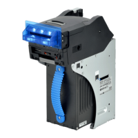
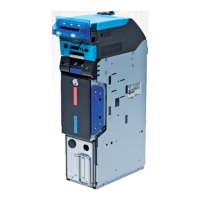
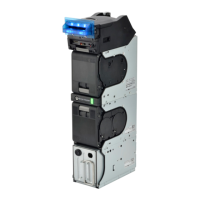
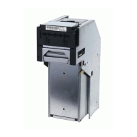
Detailed technical specifications including acceptance rate and speed.

Environmental, Electrical, and Structural Specifications

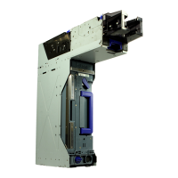
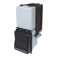
Operating conditions, power requirements, and physical specs.

Technical Contact Information

Contact details for technical support by region.

INSTALLATION

Installation Process and Grounding

General steps for installation and proper electrical grounding.

DIP Switch and Interface Configurations

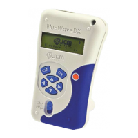
Settings for unit operation, interfaces, and DIP switches.

Sub Board 1: Connector Pin Assignments

Pinout details for Sub Board 1 USB connector.

Sub Board 1: Photo-Coupler Isolation Pin Assignment

Pinout details for Sub Board 1 Photo-Coupler Isolation.

Sub Board 1: RS232C Connector Pin Assignment

Pinout details for Sub Board 1 RS232C connector.

Sub Board 1: TTL Connector Pin Assignment

Pinout details for Sub Board 1 TTL connector.

Sub Board 2: USB Connector Pin Assignment

Pinout details for Sub Board 2 USB connector.

Sub Board 2: Photo-Coupler Isolation Pin Assignment

Pinout for Sub Board 2 Photo-Coupler Isolation.

Sub Board 2: RS232C Connector Pin Assignment

Pinout for Sub Board 2 RS232C connector.

Sub Board 2: cc-Talk Connector Pin Assignment

Pinout for Sub Board 2 cc-Talk connector.

Sub Board 2: TTL and Bezel Connector Pin Assignments

Pinouts for Sub Board 2 TTL and CN5 Bezel connectors.

Preventive Maintenance and Cleaning Procedures

Procedures for routine maintenance and cleaning the unit.

Sub Board 1 Interface Circuit Schematics

Diagrams illustrating Sub Board 1 interface circuits.

Sub Board 1: TTL and USB Schematics

Diagrams for TTL and USB interfaces on Sub Board 1.

Sub Board 2 Interface Circuit Schematics

Diagrams illustrating Sub Board 2 interface circuits.

Sub Board 2: cc-Talk, TTL, USB Schematics

Diagrams for cc-Talk, TTL, and USB interfaces on Sub Board 2.

COMMUNICATIONS

DISASSEMBLY/REASSEMBLY

WIRING DIAGRAMS

CALIBRATION AND TESTING

TROUBLESHOOTING

Related product manuals