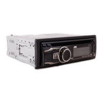
KD-SC900R
1-28 (No.49829)
SECTION 4
Description of major ICs
4.1 AK4381VT-X (IC481) : D/A converter
• Pin layout
• Block diagram
• Pin functions
MCLK
BICK
SDTI
LRCK
PDN
CSN
CCLK
CDTI
DZFL
DZFR
VDD
VSS
AOUTL+
AOUTL-
AOUTR+
AOUTR-
1
2
3
4
5
6
7
8
16
15
14
13
12
11
10
9
Pin No. Symbol I/O Description
1 MCLK I Master clock input terminal
2 BICK I Audio serial data clock terminal
3 SDTI I Audio serial data input terminal
4 LRCK I L/R Clock terminal
5 PDN I Power down mode terminal
6 CSN I Chip select
7 CCLK I Control data input terminal
8 CDTI I Control data input terminal
9 AOUTR- O Rch negative analog output terminal
10 AOUTR+ O Rch positive analog output terminal
11 AOUTL- O Lch negative analog output terminal
12 AOUTL+ O Lch positive analog output terminal
13 VSS - Connect to ground
14 VDD - Power supply terminal
15 DZFR O Rch data zero input detection terminal
16 DZFL O Lch data zero input detection terminal
De-emphasis
Control
8X
Interpolator
uP
Interface
Audio
Data
Interface
CSN
CCLK
CDTI
LRCK
BICK
SDTI
PDN
8X
Interpolator
Modulator
SCF
SCF
Clock
Divider
VDD
VSS
DZFL
DZFR
MCLK
AOUTL+
AOUTR+
AOUTR-
AOUTL-
Modulator
w
w
w
.
x
i
a
o
y
u
1
6
3
.
c
o
m
Q
Q
3
7
6
3
1
5
1
5
0
9
9
2
8
9
4
2
9
8
T
E
L
1
3
9
4
2
2
9
6
5
1
3
9
9
2
8
9
4
2
9
8
0
5
1
5
1
3
6
7
3
Q
Q
TEL 13942296513 QQ 376315150 892498299
TEL 13942296513 QQ 376315150 892498299
http://www.xiaoyu163.com
http://www.xiaoyu163.com
 Loading...