Pin No. Pin Name Description (Function)
1V
CC
Power supply (shorted with pin 30)
2 Mute ON/OFF control for all BTL AMP outputs
3V
IN
1 BTL AMP 1 input
4 VG1 BTL AMP 1 input (for gain control)
5V
O
1 BTL AMP 1 output (non-inverting side)
6V
O
2 BTL AMP 1 output (inverting side)
7 GND GND (minimum electric potential)
8 GND GND (minimum electric potential)
9 GND GND (minimum electric potential)
10 V
O
3 BTL AMP 2 output (inverting side)
11 V
O
4 BTL AMP 2 output (non-inverting side)
12 VG2 BTL AMP 2 input (for gain control)
13 V
IN
2 BTL AMP 2 input
14 REG OUT Connection for collector of external transistor (PNP); 5 V supply output
15 REG IN Connection for base of external transistor (PNP)
16 RES
Reset output
17 C
D
Reset output delay time setting (with capacitor)
18 V
IN
3 BTL AMP 3 input
19 VG3 BTL AMP 3 input (for gain control)
20 V
O
5 BTL AMP 3 output (non-inverting side)
21 V
O
6 BTL AMP 3 output (inverting side)
22 GND GND (minimum electric potential)
23 GND GND (minimum electric potential)
24 GND GND (minimum electric potential)
25 V
O
7 BTL AMP 4 output (inverting side)
26 V
O
8 BTL AMP 4 output (non-inverting side)
27 VG4 BTL AMP 4 input (for gain control)
28 V
IN
4 BTL AMP 4 input
29 V
REF
Reference voltage input for level shift circuit
30 V
CC
Power supply (shorted with pin 1)
LA6541D Pin Functions
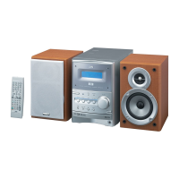
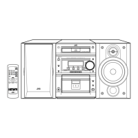
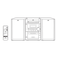
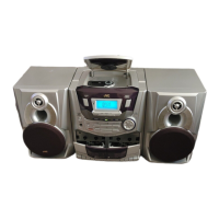
PC-X250
1 - 20
 Loading...