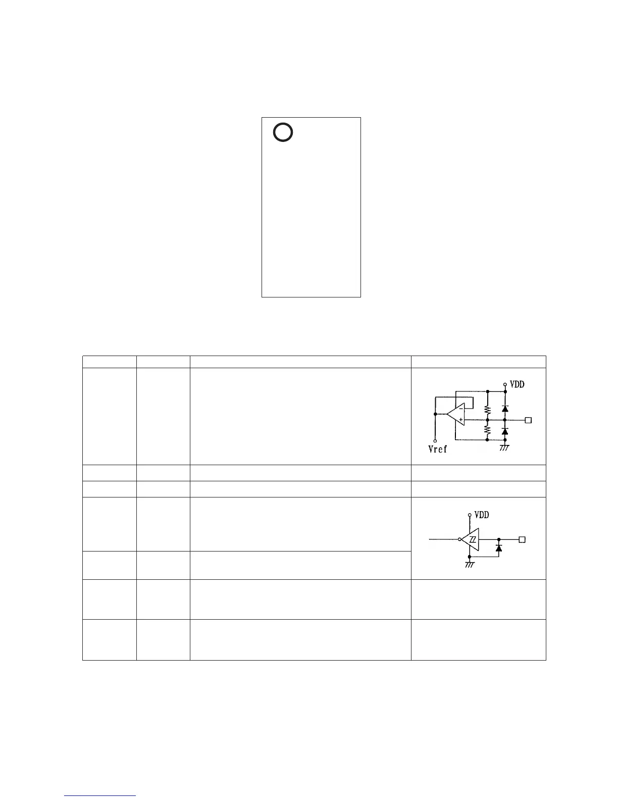
Pin No. Pin Description Notes
¥ Connection to the 0.5 ´ V
DD
voltage generator circuit used as the
analog signal ground.
Applications must connect a capacitor of about 10 µF between this pin
and V
SS
to exclude power supply ripple.
28 Vref
¥ Chip enable
Data is written to the internal latch when this pin goes from high to low.
The internal analog switches operate at this point. Data transfer is
enabled when this pin is high.
2CE
¥ Serial data and clock inputs used for IC control.
1
30
DI
CL
¥ Ground3
V
SS
¥ Power supply29
V
DD
LC75342 Pin Functions.
¥ Electronic volume and tone control testing
This pin must be tied to V
SS
during normal operation.
4
V
SS
¥ Unused.
These pins must be left open or connected to V
SS
during normal
operation.
15
16
27
NC
PC-X250
1 - 15
DI 1 30 CL
CE 2 29 VDD
VSS 3 28 VREF
TEST 4 27 NC
LOUT 5 26 ROUT
LBASS2 6 25 RBASS2
LBASS1 7 24 RBASS1
LTRE 8 23 RTRE
LIN 9 22 RIN
LSELO 10 21 RSELO
L4 11 20 R4
L3 12 19 R3
L2 13 18 R2
L1 14 17 R1
NC 15 16 NC
TOP VIEW
LC75342
LC75342 Pin Assignment
 Loading...