EasyManua.ls Logo

JVC UX-P3 User Manual

JVC UX-P3
41 pages
To Next Page IconTo Next Page
Page #1 background imageLoading...
Page #1 background image
1-1
UX-P3
SERVICE MANUAL
MICRO COMPONENT SYSTEM
No.20984
Jun. 2001
COPYRIGHT 2001 VICTOR COMPANY OF JAPAN, LTD.
UX-P3
UX-P3
Contents
Safety precautions
Preventing static electricity
Important for laser products
Disassembly method
Main adjustment
Flow of functional operation
until TOC read (CD)
Maintenance of laser pickup
Replacement of laser pickup
Description of major ICs
Internal connection of display
1-2
1-4
1-6
1-7
1-14
1-18
1-19
1-19
1-20
1-39
Area Suffix
UB
UP
US
UW
UY
Hong Kong
Korea
Singapore
South Africa
Argentina
COMPACT
DIGITAL AUDIO
CD TAPE FM/AM
MICRO COMPONENT SYSTEM UX·P3
CD-R/RW PLAYBACK
AUX
TIMER
CLOCK
STANDBY
STANDBY
/
ON
VOLUMEFUNCTION
SOUND
DIRECT OPERATING
AHB PRO
AUTO REVERSE
AUTO TAPE SELECTOR
REC
REV.MODE
PHONES
SLEEP
STANDBY/ON
AUX
FM/AM
TAPE
CD
DISPLAY
REPEATRANDOMPROG
FM MODE
AUTO
PRESET
SOUND
MODE
CD
CANCEL MULTI KEY SET
RM-SUXP3U REMOTE CONTROL
VOLUME
AHB
PRO
/
SP-UXP3 CA-UXP3 SP-UXP3
Question and Answer IconNeed help?

Do you have a question about the JVC UX-P3 and is the answer not in the manual?

JVC UX-P3 Specifications

General IconGeneral
TypeMicro Component System
TunerFM/AM
CD PlayerYes
USB PortYes
BluetoothYes
Cassette DeckNo
Speakers2 speakers included
Weight3.5 kg
Speaker Configuration2-way
FunctionsCD, USB, Bluetooth, Tuner
CD Player TypeSingle CD Player

Summary

Safety Precautions

Safety Precautions (U.K only)

Specific safety precautions for the United Kingdom market.

Preventing Static Electricity

Measures to prevent damage from electrostatic discharge (ESD) during repairs.

Important for Laser Products

Disassembly Method

Removing the Metal Cover

Steps to remove the main metal cover of the unit.

Removing the Rear Cover

Steps to remove the rear cover after the metal cover.

Removing the Tuner Board

Procedure for disconnecting and removing the tuner board.

Removing the CD Mechanism Assembly

Steps to disconnect and remove the CD mechanism assembly.

Remove the Rear Panel

Procedure for removing the rear panel.

Removing the Fan

Steps to disconnect and remove the cooling fan.

Removing the Main Board / Heat Sink

Procedure for removing the main board and heat sink.

Removing the Power Transformer Assembly

Steps to disconnect and remove the power transformer.

Removing the Front Panel Assembly

Procedure for removing the front panel assembly.

Removing the Display Board / Switch Board

Steps to remove the display and switch boards.

Removing the Headphone Board

Procedure for removing the headphone board.

Removing the Cassette Mechanism Assembly

Steps to open the cassette door and remove the mechanism.

Main Adjustment

Arrangement of Adjusting Position

Diagrams showing adjustment points for cassette mechanism and AMP board.

Tape Recorder Section

Confirmation items and methods for tape recorder adjustments.

Electrical Performance

Confirmation items and methods for electrical performance adjustments.

Flow of Functional Operation until TOC read (CD)

Maintenance of Laser Pickup

Replacement of Laser Pickup

Procedure for replacing the laser pickup unit.

Description of Major ICs

UPD780058 (IC931) : Main micon

Pin layout and functions for the main microcontroller.

LA6541 (IC801) : Foucus & Spindle & Feed & Tracking BTL driver

Pin layout and functions for the BTL driver IC.

MN662748RPM (IC651) : Digital servo & digital signal processer

Pin layout and functions for the digital servo processor.

BA15218F-XE (IC904) : Dual operation amplifier

Pin layout and block diagram for the dual op-amp IC.

KIA78S06P-T (IC933) : Regulator

Pin layout and block diagram for the regulator IC.

LA4628 (IC905) : Power amp

Pin layout and block diagram for the power amplifier IC.

AN22000A(IC601):RF & SERVO AMP

Pin layout and functions for the RF & Servo AMP IC.

LA1838 (IC1): FM AM IF AMP&detector, FM MPX decoder

Block diagram and pin functions for the FM/AM decoder IC.

LC72136N (IC2) : PLL frequency synthesizer

Pin layout, block diagram, and functions for the PLL synthesizer.

LC72723(IC3):RDS

Pin assignment, block diagram, and functions for the RDS IC.

LB1641 (IC802) : DC Motor driver

Pin layout and functions for the DC motor driver IC.

BU4094BC(IC33):Serial to parallel port extension

Pin layout and block diagram for serial-to-parallel converter.

BA3126N(IC31) : R/P Switch

Diagram for the record/playback switch IC.

GP1U26X (IC933)

Diagram for the GP1U26X IC.

NJU6433FG1 (IC934)

Pin layout, block diagram, and functions for the NJU6433FG1 IC.

LC75345M (IC901)

Pin layout and block diagram for the LC75345M IC.

AN7317 (IC32) : PB/REC amp

Block diagram and pin descriptions for the PB/REC amp IC.
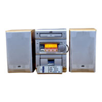
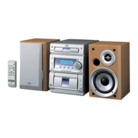
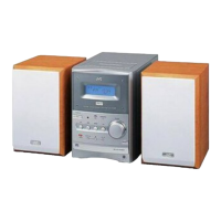
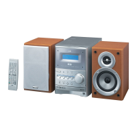
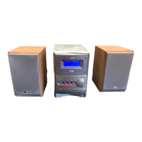
Internal connection of display QLD0160-001 (D1934)

Related product manuals