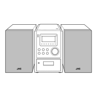
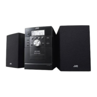
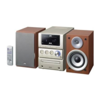
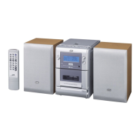
UX-M3R
1-22
Symbol I/OPin No. Symbol I/O Function
51
52
53
54
55
56
57
58
59
60
61
62
63
64
65
66
67
68
69
70
RFGC
TEBC
FMO
FVO
DMO
2VREF
SEL
FLGA
FLGB
FLGC
FLGD
VDD3
VSS3
IO0
IO1
IO2
IO3
DMOUT
CKSE
DACT
RF amplitude adjustment control signal output
terminal.
Tracking balance control signal output terminal.
Feed equalizer output terminal.
Speed error signal or feed search equalizer
output terminal.
Disk equalizer output terminal. (PWM carrier=
88.2kHz for DSP, Synchronize to PXO)
Analog double reference voltage supply
terminal.
APC circuit ON/OFF indication signal output
terminal. At the laser on time, UHF = L at "HiZ"
level and UHF = H at "H" level.
External flag output terminal for internal
signal. Can select signal from TEZC, FOON,
FOK and RFZC by command.
External flag output terminal for internal
signal. Can select signal from DFCT, FOON,
FMON and RFZC by command.
External flag output terminal for internal
signal. Can select signal from TRON, TRSR,
FOK and SRCH by command.
External flag output terminal for internal
signal. Can select signal from TRON, DMON,
HYS and SHC by command.
Digital power supply voltage terminal.
Digital ground terminal.
General I/O terminal. Can change over input
port or output port by command. At the input
mode time can readout a state of terminal (H/L)
by read command. At the output mode time can
control a state of terminal (H/L/HiZ) by
command.
This terminal controls IO0~IO3 terminal.
At "L" level time, IO0, 1 out feed equalizer
signal of 2-state PWM, IO2,3 out disk equalizer
signal of 2-state PWM.
Normally, keep at open.
DAC test mode terminal. Normally, keep at
open.
O
O
O
O
O
-
O
O
O
O
O
-
-
I/O
I/O
I/O
I/O
I
I
I
71
72
73
74
75
76
77
78
79
80
81
82
83
84
85
86
87
88
89
90
91
92
93
94
95
96
97
98
99
100
TESIN
TESIO1
VSS4
PXI
PXO
VDD4
XVSS
XI
XO
XVDD
DVSR
RO
DVDD
DVR
LO
DVSL
TEST1
TEST2
TEST3
BUS0
BUS1
BUS2
BUS3
VDD5
VSS5
BUCK
CCE
TEST4
TSMOD
RST
Test input terminal. Normally, keep at "L" level.
Test input/output terminal. Normally, keep at
"L" level.
Digital ground terminal.
Crystal oscillator connecting input terminal for
DSP. Normally, keep at "L" level.
Crystal oscillator connecting output terminal
for DSP.
Digital power supply voltage terminal.
Oscillator ground terminal for system clock.
Crystal oscillator connecting input terminal for
system clock.
Crystal oscillator connecting output terminal
for system clock.
Oscillator power supply voltage terminal for
system clock.
Analog ground terminal for DA converter.(R-ch)
R channel data forward output terminal.
Analog supply voltage terminal for DA
converter.
Reference voltage terminal for DA converter.
L channel data forward output terminal.
Analog ground terminal for DA converter.(L-ch)
Test mode terminal. Normal, keep at open.
Test mode terminal. Normal, keep at open.
Test mode terminal. Normal, keep at open.
Micon interface data input/output terminal.
Digital power supply voltage terminal.
Digital ground terminal.
Micon interface clock input terminal.
Command and data sending/receiving chip
enable signal input terminal.
The bus line becomes active at "L" level.
Test mode terminal. Normal, keep at open.
Local test mode selection terminal.
Reset signal input terminal. Reset at "L" level.
I
I
-
I
O
-
-
I
O
-
-
O
-
-
O
-
I
I
I
I/O
I/O
I/O
I/O
-
-
I
I
I
I
I
Pin No. Function
 Loading...