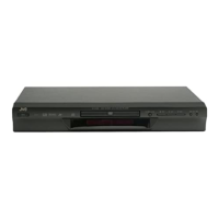
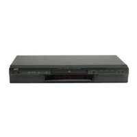
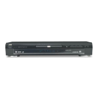
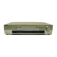
XV-S300BK/XV-S332SL/XV-S402SL/XV-S403SG
42
4.17.3 Pin function (ZIVA-4.1-PB0 : 2/5)
Pin No. Symbol I/O Description
37 VSS - Connect to ground
38 NC - Non connect
39 NC - Non connect
40 NC - Non connect
41 NC - Non connect
42 NC - Non connect
43 PIO0 I/O Programmable I/O terminal
44 VSS - Connect to ground
45 VDD_3.3 - Power supply terminal 3.3V
46 PIO1 I/O Programmable I/O terminal
47 PIO2 I/O Programmable I/O terminal
48 PIO3 I/O Programmable I/O terminal
49 PIO4 I/O Programmable I/O terminal
50 PIO5 I/O Programmable I/O terminal
51 PIO6 I/O Programmable I/O terminal
52 PIO7 I/O Programmable I/O terminal
53 MDATA0 I/O SDRAM data
54 MDATA1 I/O SDRAM data
55 VDD_3.3 - Power supply terminal 3.3V
56 VSS - Connect to ground
57 MDATA2 I/O SDRAM data
58 MDATA3 I/O SDRAM data
59 MDATA4 I/O SDRAM data
60 MDATA5 I/O SDRAM data
61 MDATA6 I/O SDRAM data
62 MDATA7 I/O SDRAM data
63 MDATA15 I/O SDRAM data
64 VDD_3.3 - Power supply terminal 3.3V
65 VSS - Connect to ground
66 MDATA14
I/O SDRAM data
67 VDD_2.5 - Power supply terminal 2.5
68 VSS - Connect to ground
69 MDATA13 I/O SDRAM data
70 MDATA12 I/O SDRAM data
71 MDATA11 I/O SDRAM data
72 MDATA10 I/O SDRAM data
73 MDATA9 I/O SDRAM data
74 VDD_3.3 - Power supply terminal 3.3V
75 VSS - Connect to ground
76 MDATA8 I/O SDRAM data
77 LDQM O SDRAM Lower or upper mask
78 SD-CLK O SDRAM Clock
79 CLKSEL I Selects SYSCLK or VCLK as clock source. Normal operation is to tie HIGH.
80 MADDR9 O SDRAM address
81 MADDR8 O SDRAM address
82 VDD_3.3 - Power supply terminal 3.3V
83 VSS - Connect to ground
84 MADDR7 O SDRAM address
 Loading...