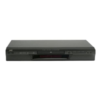
XV-S300BK/XV-S332SL/XV-S402SL/XV-S403SG
43
4.17.4 Pin function (ZIVA-4.1-PB0 : 3/5)
Pin No. Symbol I/O Description
85 MADDR6 O SDRAM address
86 MADDR5 O SDRAM address
87 VDD_2.5 - Power supply terminal 2.5V
88 VSS - Connect to ground
89 MADDR4 O SDRAM address
90 MWE
O SDRAM write enable
91 SD-CAS
O Active LOW SDRAM column address
92 VDD_3.3 - Power supply terminal 3.3V
93 VSS - Connect to ground
94 SD-RAS
O Active LOW SDRAM row address
95 SD-CS0
O Active LOW SDRAM chip select 0
96 SD-CS
/MADDR11
O Active LOW SDRAM chip select 1 or use as MADDR11 for larger SDRAM
97 SD-BS
O SDRAM bank select
98 MADDR10 O SDRAM address
99 MADDR0 O SDRAM address
100 VDD_3.3 - Power supply terminal 3.3V
101 VSS - Connect to ground
102 MADDR1 O SDRAM address
103 MADDR2 O SDRAM address
104 MADDR3 O SDRAM address
105 RESERVED I Tie to VSS or VDD_3.3 as specified in table 1
106 NC - Non connect
107 NC - Non connect
108 RESERVED I Tie to VSS or VDD_3.3 as specified in table 1
109 NC - Non connect
110 RESERVED I Tie to VSS or VDD_3.3 as specified in table 1
111 RESERVED I Tie to VSS or VDD_3.3 as specified in table 1
112 RESERVED I Tie to VSS or VDD_3.3 as specified in table 1
113 DAI-LRCK I PCM left/right clock
114 DAI-BCK I PCM input bit clock
115 VDD_3.3 - Power supply 3.3V
116 VSS - Connect to ground
117 DAI-DATA I PCM data input
118 DA-DATA3 O PCM data output. Eight channels. Serial audio samples relative to
DA_BCK and DA_LRCK
119 DA-DATA2 O PCM data output. Eight channels. Serial audio samples relative to
DA_BCK and DA_LRCK
120 DA-DATA1 O PCM data output. Eight channels. Serial audio samples relative to
DA_BCK and DA_LRCK
121 DA-DATA0 O PCM data output. Eight channels. Serial audio samples relative to
DA_BCK and DA_LRCK
122 DA-LRCK O PCM left clock. Identifies the channel for each sample
123 VDD_3.3 - Power supply terminal 3.3V
124 VSS - Connect to ground
125 DA-XCK I/O Audio external frequency clock input or output
126 DA-BCK O PCM bit clock output
127 DA-IEC O PCM data out in IEC-958 format or compressed data out in IEC-1937 format
128 VDD_2.5 - Power supply terminal 2.5V
 Loading...