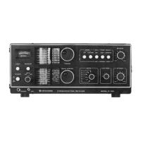
R-2000
CIRCUIT
DESCRIPTION
Item
Rating
Center frequency
455
kHz
± 0.6 kHz
6 dB band
width
2.s
±0.3
kHz
40
dB band
width
5.5 kHz
or
less
Insertion loss (at maximum output)
6.0 dB
or
less
Guaranteed attenuation
55
dB
or
more
(within
455
±
100
kHz)
,
Spurious attenuation
(within
0.1
to
1.0 MHz)
45
dB
or
more
for
600
to
700
kHz.
40
dB
or
more
1/0 matching impedance
2.0
k.Q
Table 2. Ceramic filter {L72-0332-05, RX unit F3)
SSS,
AM-N,
CW-W
Item
Rating
Nominal center frequency
455
kHz
6 dB band
width
± 3
kHz
or
more
(from
455
kHz)
50
dB band width
± 9 kHz
or
less (from
455
kHz)
Ripple (within
455
± 2
kHz)
2 dB
or
less
Insertion loss
6 dB or less
Guaranteed attenuation
60
dB
or
more
(within
455
±
100
kHz)
1/0 matching impedance
2.0
k.Q
Table 3. Ceramic filter (L72-0319-05, RX unit F4)
AM-W
Item Rating
Nominal center frequency
455
kHz
6 dB bandwidth
± 7 .5 kHz
or
more
50 dB bandwidth
± 15 kHz
or
less
Ripple (within
455
± 5
kHz)
3 dB
or
less
Loss 6
dB
or
less
Guaranteed attenuation
35 dB or more
(within
455
±
100
kHz)
Input and output impedance 1.5
k.Q
Table
4.
Ceramic filter (L72-0316-05, RX unit F5)
FM
Item
Rating
Center frequency
fo
455.7
kHz
Center frequency deviation
fo
±50
Hz at 6 dB
6 dB bandwidth
±250
Hz
or
more
60
dB bandwidth
±425
Hz
or less
Ripple
2 dB or less
Loss
6 dB or less
80dB
or more
Guaranteed attenuation
at
100
Hz
to 455. 1 kHz and
456.3 kHz to 2 MHz
lmput
and
output impedance
2kQ#'15
pF
Table 5.
CW
Crystal filter (L71-0206-05)
YG-455C
(Option)
4
Item
Rating
Center frequency quency f o 455.7 kHz
Center frequency deviation
Jo
±50Hzat6dB
6 dB bandwidth
± 1 25
Hz
or more
60
dB bandwidth
±
250
Hz
or less
Ripple
2 dB
or
less
Loss
6 dB or less
80
dB
or
more at
Guaranteed attenuation
100
Hz
to
455.3
kHz and
456.1 kHz
to
2 MHz
Input and output impedance
2
k.Q
//
15
pF
Table 6.
CW
Crystal filter
(l71-0207-05)
YG-455CN
(Option)
PLL
(Phase locked
loop)
unit
XS0-1920-00
The
PLL
unit houses the PU. oscillator circuit, microproces-
sor control circuit and the
NB
amplifier circuits.
In
the
PLL
circuit, there
is
a 9 MHz reference frequency crystal oscilla-
tor, the first local oscillator (45.90
,...,
75.85
MHz), second
local oscillator (36 MHz) and third local oscillator (9.395
,...,
9.445
MHz),
which are output to the Receiver unit.
The
digital circuit peripheral to the microprocessor controls
the
PLL
circuit frequency, display, clock/timer, input inter-
face, rotary encoder mode (speed) and memory.
1 . PLL circuit
1 ) Reference frequency oscillator
01
operates at a reference frequency of 9 MHz, which
is
supplied to the second and third local oscillator cir-
cuits through buffer
02.
Via
buffer
03,
a 4.5 MHz signal divided 1
/2
by
IC
1
is
supplied through buffer
04
to the first local oscillator
PLL
circuit.
The
reference frequency
is
also buffered
(06) and divided down to 1
kHz
by IC2 for use
as
a
clock reference signal.
2)
First local oscillator circuit
(LO
1)
The
first local oscillator
is
obtained from the
PLL
(Phase Locked Loop) circuit. Three
VCOs
(Voltage
Controlled Oscillator) controlled by the microproces-
sor through
020
,..,
22
cover the
45.90
,...,
75.85
MHz frequency range. The
VCO
output
is
amplified by
026.
027
and
028.
Part of the signal
is
applied to
buffer
016:.
2SC1907
and
PLL
IC5:
MN614
7C.
The
spurious component
is
eliminated from the remaining
signal by a
BPF
and
is
output via. buffer
029
and
030:
2SC 1
707
as
the
LO
1 signal.
IC5:
MN6147C
consists
of
a programmable fre-
quency divider. reference frequency divider and phase
comparator which compares the reference and
VCO
frequencies (comparision frequency;
25
kHz).
The
programmable divider's ratio (
1836
,..,
3034;
only
even
number)
is
controlled by the microprocessor.
The
phase error signal from the comparator
is
applied
to the
VCO
by active filter
017,
018
and
019:
2SC1775.
3)
Second local oscillator (L02)
The
reference frequency
is
quadrupled by
05:
2SC
1815
to obtain the
36
MHz second local oscilla-
tion frequency.
 Loading...