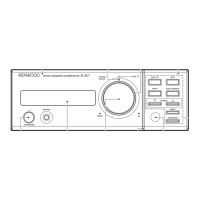
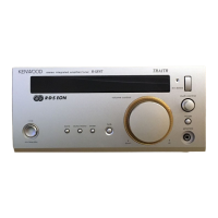
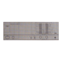
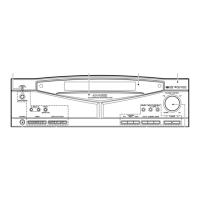
R-A100/A150/V300/V350
7
CIRCUIT DESCRIPTION
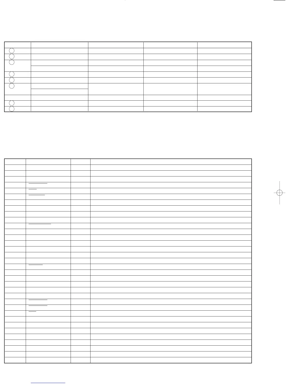
2-2 Key matrix
DSW1~DSW4 : Tuner distination
DSW5 : R-A100/A150 or R-V300/V350 Model distination
PTY,TA / NEWS / INFO / DISPLAY(RDS) : RDS function model (R-V350/A150)
( ) : R-V300 / V350 /A100 function
✣ : R-A150 (E,T type) function
2 KR3 3 KR2 4 KR1 5 KR0
73 KS0 – – – –
74 KS1 TUNING % DISPLAY(RDS) PTY TA/NEWS/INFO
75 KS2 (MULTI MODE) (MULTI LEVELfi) (MULTI LEVEL%) –
✣ CLOCK ✣ TIMER MODE ✣ TIMER SET –
76 KS3 TUNING fi AUTO MEMORY BAND AUTO
77 KS4 (VOICE ON/OFF) (TIMER SET) INPUT @ INPUT #
78 KS5 (CLOCK SET) (TIMER MODE) ON/STANDBY TAPE2(MONITOR)
✣ VOICE ON/OFF
KS6 – – – –
81 KS7 DSW1(D29) DSW2(D30) DSW3(D31) DSW4
82 KS8 – – – DSW5(D34)
2-3 Pin description
No. Name I/O Description
1 Vdd I Power supply(+5V)
2-5 KR3-0 I Key return 3-0
6,7, ENC_VOL1,2 I Encoder pulse detect1,2
8 HP_DET I Headphone detect L: Yes
9 CE I Chip enable L: Enable
10 RESET I Microprocessor reset L: Reset
11,12 X1,2 I Clock generator
13 IC(Vpp) - Connect to Vss
14,15 XT1,2 - Sub clock generator
16 Vdd - Power supply(+5V)
17 HP_MUTE O Mute of headphones
18 PROTECTION I Protection detection
19 SBUSY I/O Serial data busy
20 SDATA I/O Serial data
21 DSP_CLK O Clock for DSP
22 DSP_DATA O Data for DSP
23 DSP_ST O Strobe for DSP
24 MUTE O Mute control L: Mute ON
25 Avss - GND of A/D converter
26 PLL_DO O PLL DO
27 PLL_CE O Chip enable for PLL
28 PLL_DATA O Data detection for PLL
29 PLL_CLK O Clock for PLL
30 T_MUTE O Mute for tuner L: Mute ON
31 STEREO I Stereo signal detection L: Stereo
32 SD I Synchro signal detection L: SD detection
33 RDS_SLEVEL I Signal level of RDS
34 Avdd - Analog power supply for A/D converter
35 Avref - Reference voltage for A/D converter
36 RDS_CLK I Clock for RDS
37 RDS_DATA I Data for RDS
38 N.C. I No used
39 REMOCON_IN I Input port of remote control signal
40 Vss - GND
R-A100/V300(k)1P 98.4.25 11:35 y[W 14
 Loading...