VCO
UNlT
(X50-1370-10)
The VCO is a Colpitts type oscillating circuit (07)
and its frequency varies with the control voltage applied to
varicap diode Dl. This circuit is strictly stabilized against
changes in temperature and power source voltage to im-
prove the C/IU of its output and prevent unlocking.. The
VCO's output is passed through buffer 06, amplified by
012 and applied to MIX through D6 and D7 for both
reception and transmission.
In the LOCAL OSC, two quartz crystals for
0 and 5
kHz are switched with a switching diode. 08 performs over-
tone oscillation and its output is tripled in 09 to 127.930
and 127.935 MHz which are applied to MIX stage. The
lMlX circuit mixes the output and the VCO's output ampli-
fied by 05, and its output is passed through a .rr-type LPF
to deliver IF output of 5.37
-
9.36 MHz.
The output is amplified by the wide-band amplifier
of
01 to 03 and applied to the programmable counter.
013, which turns on and off VCO amp 012, is a protective
circuit in order to prevent emission of spurious radiation
occurring when the PLL circuit fails to lock and the VCO
runs away. This circuit
is
automatically reset when the
PLL begins to work properly because
it
is not involved in
the phase lock loop. D8 provides a certain time delay
when 013 is turned off, so 013 does not operate during
the transient state before the VCO is locked, though the
indicator works. This contributes to reduce noise.
PD
UNlT
(X50-1380-10)
06 serves as the interface and buffer amp for IC8.
The waveform of its IF output is shaped in IC8 and its
output frequency is divided to 10 kHz by the program-
mable counter consisting of IC5 to 12 and the resulting
signal is applied to MC4044P of IC4. While IC1 generates
5.12 MHz signal which is divided .to 112 by the flip-flop
circuit involved in IC1. The resulting frequency is further
divided to 1/16 in IC2, IC3 and 10-kHz output signal is'
applied to MC4044P of IC4.
-
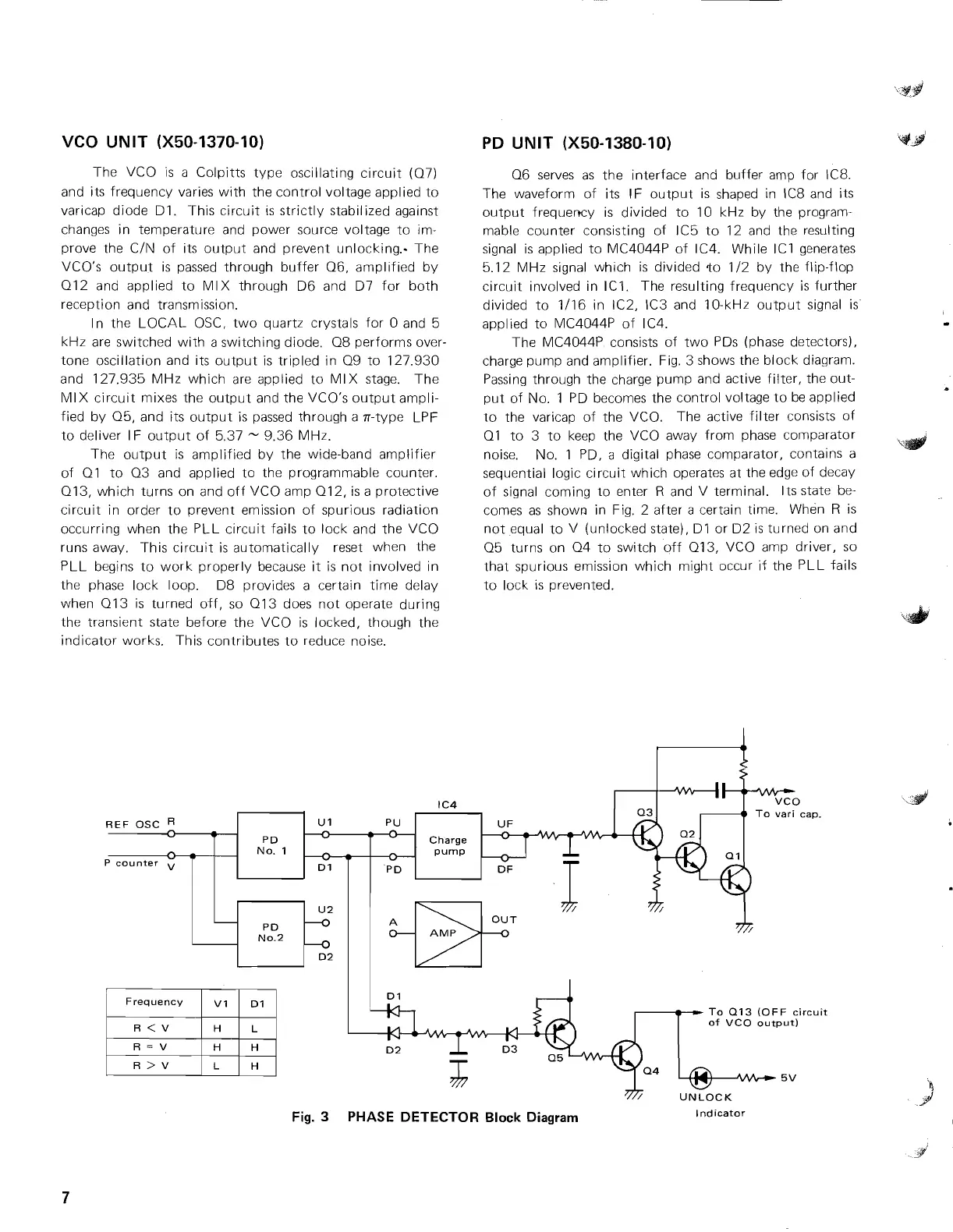
The MC4044P consists of two PDs (phase detectors),
charge pump and amplifier. Fig. 3 shows the block diagram.
Passing through the charge pump and active filter, the out-
put of No. 1 PD becomes the control voltage to be applied
to the varicap of the VCO. The active filter consists of
01 to 3 to keep the VCO away from phase comparator
vd
noise. No. 1 PD, a digital phase comparator, contains a
sequential logic circuit which operates at the edge of decay
of signal coming to enter
R
and V terminal. Its state be-
comes as shown in Fig. 2 after a certain time. When
R
is
not equal to V (unlocked state), Dl or D2 is turned on and
05 turns on 04 to switch off 013, VCO amp driver, so
that spurious emission which might occur if the
PLL fails
to lock is prevented.
w
I
C4 VCO
0
To vari cap.
REF
OSC
U
1
PU U F
-
m
-
r\
"
-
V
-"
PD
Charge
w
fi
-
No.
1
A
pump
P--
Dl
w
-
w
w
PD D F
No.2
;
-
To
013 (OFF
circuit
of
VCO
output)
04
5
v
UNLOCK
Fig.
3
PHASE DETECTOR
Block
Diagram
Indicator