A
Anthony ManningSep 10, 2025
How to fix incorrect screen display during power up on my Kenwood TS-990S?
- EElizabeth WattsSep 10, 2025
If screens do not appear correctly during power up, reset the transceiver.


How to fix incorrect screen display during power up on my Kenwood TS-990S?
If screens do not appear correctly during power up, reset the transceiver.
How to fix no audio from the speaker on my Kenwood TS-990S?
If there's no audio from the speaker, first, rotate the AF control clockwise and the SQL control counterclockwise. Ensure headphones are disconnected. If in FM mode, deactivate CTCSS. Also, unmute the audio line and check the external speaker connection and configuration, disconnecting it to test if necessary.
What to do if the audio is distorted on my Kenwood Transceiver?
Audio distortion can occur if the AGC function is active; try enabling it or adjusting the RF gain with the RF control. It can also be caused by a high audio level, so rotate the AF control to adjust the volume level.
Why can't I receive signals on my Kenwood TS-990S Transceiver even with the antenna connected?
If you cannot receive and the RX sensitivity is low, start by adjusting the SQL control and ensuring the DCD LED on the TNC is not lit. Disable the attenuator and preamplifier. Make sure the RX ANT is inactive and reselect the antenna. If antenna tuning is the issue, press and hold [AT/TUNE] to tune or stop the antenna tuning. Rotate the RF control fully clockwise, reset the center frequency of the preselector to default, and ensure the transverter is correctly configured and working properly. Review the configuration for the additional filter and readjust the preselector (main band only).
What to do if my Kenwood TS-990S does not transmit and the PWR meter is inactive?
If the transceiver doesn't transmit and the PWR meter is inactive, unlock the PTT switch if it's locked on while using a stand microphone. Ensure the selected frequency is within the amateur band. Disable TX Inhibit in Menu 6-03.
How to fix distorted or clipped audio reports on my Kenwood TS-990S?
If another station reports distorted or clipped audio, adjust the microphone gain and the input level of the speech processor. Use the transmit monitor function or have the other station monitor while you make these adjustments.
How to fix insufficient modulation in FM mode on my Kenwood Transceiver?
If modulation is insufficient in FM mode, review the configuration for Microphone Gain in Advanced Menu 13.
Why is the S meter performance dull in FM mode on my Kenwood Transceiver?
If the S meter performance is dull in FM mode, select 'High' for the S meter sensitivity in Menu 0-08.
What to do if the linear amplifier does not behave with my Kenwood Transceiver?
If the linear amplifier is not working, securely connect the amplifier to the REMOTE connector. Review the configuration for Data VOX and the input signal level. Select 'Active High + Relay Control' for the linear amplifier control from Advanced Menu 11.
How to troubleshoot VOX function issues on my Kenwood Transceiver?
If the VOX function isn't working correctly, adjust the VOX gain level. If the VOX gain level is too high, adjust the Anti VOX Gain level.
Rotate the dial portion of the main knob ASSY clockwise to its maximum position (torque OFF), then attach the main knob ASSY to the panel.
Forming the two coaxial cables (E37-1570-05, E37-1571-15) as shown in the figure.
Description of the main receiver block.
Explanation of the reference signal generator.
Description of MLO1 and MLO2 local oscillators.
Frequency configuration for transmission and sub-receiver.
Description of TLO1, SLO1, SLO2, and SLO3 local oscillators.
Explanation of the noise detector circuit.
Signal path from antenna terminal to sub preamplifier.
Description of the 1st mixer.
Explanation of the noise blanking circuit.
Signal path from TIF to drive output.
Explanation of antenna tuner and protections.
Signal path from IF input to IF amplifier.
Signal path from 2nd mixer to 3rd mixer input.
Details on the main MCU and its periphery.
Details on the scope MCU and its periphery.
Details on application MCUs and their periphery.
Communication between main MCU and application MCU.
Communication between application MCU and scope DSP.
Communication with the panel MCU.
Description of the LAN interface circuit.
Circuits around the panel MCU.
Explanation of the touch panel.
Description of the LCD backlight controller.
Details on LEDs for main and sub displays.
Parts list for the accessory unit.
Pinout and function for the Main MCU.
Pinout and function for IC42.
Pinout and function for IC43.
Pinout and function for IC32.
Pinout and function for IC33.
Pinout and function for IC34.
Pinout and function for IC36.
Pinout and function for IC37.
Pinout and function for IC38.
Pinout and function for IC39.
Pinout and function for the Main MCU.
Pinout and function for the Scope MCU.
Pinout and function for TXMRX-DSP.
Pinout and function for SRX-DSP.
Diagnosing faults in BGA ICs.
List of BGA parts requiring service.
Procedures for checking power supply voltages.
Procedures for checking clock signals.
Checking Reset/LCDREQ signal inputs.
Checking main display communication waveforms.
Checking sub display communication waveforms.
Instructions for updating the firmware.
List of necessary test equipment for adjustments.
Preparation steps before starting adjustments.
Description of the service jig.
Details on the ACC 2 connector short plug.
Instructions for using the ACC 2 connector short plug.
Details on the adjustment rod.
Method for using the adjustment rod.
Details on the jig cable.
Outline of the adjustment mode.
Steps to start the adjustment mode.
Steps for setting and performing a full reset.
Checks for LCD and LED functionality.
Procedure for adjusting main reference lock voltage.
Procedure for adjusting main VCO3 lock voltage.
Procedure for adjusting main VCO4 lock voltage.
Procedure for adjusting sub LO2 level.
Procedure for adjusting sub reference lock voltage.
Procedure for adjusting sub LO1 level.
Procedure for adjusting TX VCO1 lock voltage.
Procedure for adjusting TX VCO2 lock voltage.
Procedure for adjusting TX VCO3 lock voltage.
Procedure for adjusting TX VCO4 lock voltage.
Adjustment for MAIN RX trap frequency.
Adjustment for the 1st mixer balance.
Adjustment for MAIN RX 1st IF notch.
Adjustment for HF BPFs.
Adjustment for SUB RX IF trap frequency.
Adjustment for SUB RX trap frequency.
Adjustment for SUB RX HF BPF.
Adjustment for MAIN RX 1st mixer balance.
Adjustment for MAIN RX 1st IF notch.
Adjustment for MAIN RX HF BPF notch.
Adjustment for SUB RX trap frequency.
Adjustment for SUB RX HF BPF.
Adjustment for IF filters.
Adjustment for NB MCF (15kHz).
Adjustment for carrier point.
Adjustment for SUB RX 1st mixer balance.
Adjustment for SUB RX trap frequency.
Adjustment for SUB RX HF BPF.
Adjustment for SUB RX HF BPF.
Adjustment for SUB RX MCF.
Adjustment for SUB RX NB voltage.
Adjustment for SUB RX FM discriminator.
Adjustment for SUB RX carrier point.
Adjustment for MAIN RX AGC start level.
Adjustment for MAIN RX AGC start level.
Adjustment for MAIN RX AGC start level.
Adjustment for MAIN RX AGC gain curve.
Adjustment for MAIN RX SSB S-meter.
Adjustment for MAIN RX HF FM S-meter.
Adjustment for MAIN RX 50M FM SQL threshold.
Adjustment for MAIN RX 50M FM SQL tight.
Adjustment for SCOPE gain.
Adjustment for MAIN RX 50M FM S-meter.
Adjustment for SUB RX NB voltage.
Adjustment for SUB RX AGC start level.
Adjustment for SUB RX AGC start level.
Adjustment for SUB RX AGC start level.
Adjustment for SUB RX AGC start level.
Adjustment for SUB RX AGC gain curve.
Adjustment for SUB RX SSB S-meter.
Adjustment for SUB RX 50M FM S-meter.
Adjustment for SUB RX 50M FM S-meter.
Procedure for checking MAIN RX S/N.
Procedure for checking SUB RX S/N.
Check for simultaneous main and sub RX.
Adjustment for MAIN PRE-AMP gain.
Adjustment for MAIN RF ATT.
Adjustment for SUB RF ATT.
Adjustment for MAIN NB gain.
Adjustment for SUB NB gain.
Adjustment for ALC reference voltage.
Adjustment for TX IF gain.
Procedure for checking TX IF gain.
Check for TX HF BPF (49~54M).
Adjustment for final idling current.
Procedure for checking fan operation.
Procedure for checking Vd meter.
Setting the ID current.
Procedure for checking power output.
Adjustment for protection circuits.
Adjustment for SWR meter.
Adjustment for AT check.
Procedure for checking SWR meter.
Adjustment for AT check.
Adjustment for HF POC 200W.
Procedure for checking power meter 200W.
Adjustment for 50M POC 200W.
Procedure for checking 50M power meter 200W.
Adjustment for HF POC 100W.
Procedure for checking power meter 100W.
Adjustment for HF POC 50W.
Procedure for checking power meter 50W.
Adjustment for HF POC 25W.
Procedure for checking power meter 25W.
Adjustment for HF POC 10W.
Procedure for checking power meter 10W.
Adjustment for HF POC 5W.
Adjustment for FM deviation.
Adjustment for SCOPE gain.
Adjustment for HF TGC.
Adjustment for HF PGC.
Adjustment for FM deviation.
Adjustment for protection circuits.
Adjustment for protection circuits.
Adjustment for SWR meter.
Adjustment for AT check.
Procedure for checking SWR meter.
Adjustment for AT check.
Adjustment for HF POC 200W.
Procedure for checking power meter 200W.
Adjustment points on the final unit.
Adjustment points on the AT unit.
Adjustment points on the PLL main unit.
Adjustment points on the PLL sub unit.
Adjustment points on the RX unit.
Adjustment points on the RX unit.
Adjustment points on the TX-RX unit.
Adjustment points on the TX-RX unit.
Pinout and function for the SCOPE accessory unit.
Pinout and function for the PRESEL accessory unit.
Pinout and function for the MIC accessory unit.
Pinout and function for the USB accessory unit.
Pinout and function for the PHONES/PADDLE accessory unit.
Pinout and function for the accessory POW SW unit.
Pinout and function for the MULTI accessory unit.
Pinout and function for the HC/LC accessory unit.
Pinout and function for the NR/NB accessory unit.
Pinout and function for the NOTCH/SQL accessory unit.
Pinout and function for the DC-DC unit.
Pinout and function for the DC-DC unit.
Pinout and function for the DC-DC unit.
Pinout and function for the DC-DC unit.
Pinout and function for the DC-DC unit.
Pinout and function for the DC-DC unit.
Pinout and function for the TX-RX unit.
Pinout and function for the RX BPF unit.
Pinout and function for the TX-RX unit.
Pinout and function for the TX-RX unit.
Pinout and function for the main display unit.
Pinout and function for the sub LCD unit.
Pinout and function for the main display unit.
Pinout and function for the sub LCD unit.
Pinout and function for the PLL main unit.
Pinout and function for the PLL sub unit.
Pinout and function for the AT unit.
Pinout and function for the AT unit.
Pinout and function for the control unit.
Pinout and function for the control unit.
Pinout and function for the control unit.
Pinout and function for the digital unit.
Pinout and function for the DSP unit.
Pinout and function for the main display unit.
Pinout and function for the sub LCD unit.
Pinout and function for the main display unit.
Pinout and function for the sub LCD unit.
Pinout and function for the main display unit.
Pinout and function for the sub LCD unit.
Pinout and function for the main display unit.
Pinout and function for the sub LCD unit.
Pinout and function for the main display unit.
Pinout and function for the main display unit.
Pinout and function for the AF/RF display unit.
Pinout and function for the sub LCD unit.
Pinout and function for the RX unit.
Pinout and function for the RX BPF unit.
Pinout and function for the TX-RX unit.
Pinout and function for the TX-RX unit.
Pinout and function for the TX-RX unit.
Pinout and function for the TX-RX unit.
A section for notes and remarks.
Level diagram for the main band receiver section.
Level diagram for the sub band receiver section.
Level diagram for the transmitter section.
Information on ARCP-990 Radio Control Program.
Information on ARHP-990 Radio Host Program.
Specifications for the SP-990 external speaker.
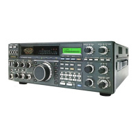
General specifications of the transceiver.
Transmitter specifications.
Receiver specifications.
| Receiver Type | Triple Conversion Superheterodyne |
|---|---|
| Antenna Tuner | Built-in automatic antenna tuner |
| DSP | Yes |
| IF DSP | Yes |
| Modes | SSB, CW, AM, FM |
| Display | 7-inch TFT color LCD |
| Weight | 25 kg (55.1 lbs) |
| Antenna Connectors | SO-239 |
| Power Supply | 13.8V DC |