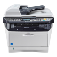
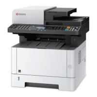
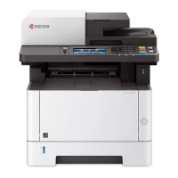
2PK/2PL/2PM/2PN
2-3-7
YC8 17 CCDPH2P O LVDS CCD shift register clock signal (-)
Connected to
the CCD
PWB
18 CCDPH2N O LVDS CCD shift register clock signal (+)
19 NC - - Not used
20 CCDSH O LVDS CCD shift gate signal (-)
21 CCDSW O LVDS CCD color/BW change signal (+)
22 GND - - Ground
23 CCDDATAR I LVDS CCD image output signal (Red)
24 GND - - Ground
25 CCDDATAG I LVDS CCD image output signal (Green)
26 GND - - Ground
27 CCDDATAB I LVDS CCD image output signal (Blue)
28 GND - - Ground
29 +12V3 O 12 V DC 12 V DC power source (For exposure
lamp)
30 GND - - Ground
31 +5V3E2 O 5 V DC 5 V DC power source
32 +5V3E2 O 5 V DC 5 V DC power source
YC9 1 GND - - Ground
Connected to
the scanner
PWB
2 +3.3V3C O 3.3 V DC 3.3 V DC power source
3 CPUCLK I 0/3.3 V DC (pulse) Serial communications clock signal
4 CPUSI I 0/3.3 V DC (pulse) Serial communications data input
5 CPUSO O 0/3.3 V DC (pulse) Serial communications data output
6 CPUSEL I 0/3.3 V DC Communications select signal
7 CPURDY O 0/3.3 V DC Communications ready signal
8 OVANOHLD O 0/3.3 V DC Communications ready signal
9 PAGESET O 0/3.3 V DC Vertical synchronizing monitor signal
10 SEGSO I 0/3.3 V DC Vertical synchronizing signal
11 SSCKN O 0/3.3 V DC (pulse) Serial communications clock
12 SEGSI O 0/3.3 V DC (pulse) Serial communications data input
13 SSBSY I 0/3.3 V DC Impossible transmission/Completion
notice signal
14 SSDIR I 0/3.3 V DC Serial communications T/R switching sig-
nal
15 SEGIR I 0/3.3 V DC Serial communications interruption
demand signal
Connector Pin Signal I/O Voltage Description
 Loading...