2T6/2T7/2T8/2T9
2-3-2
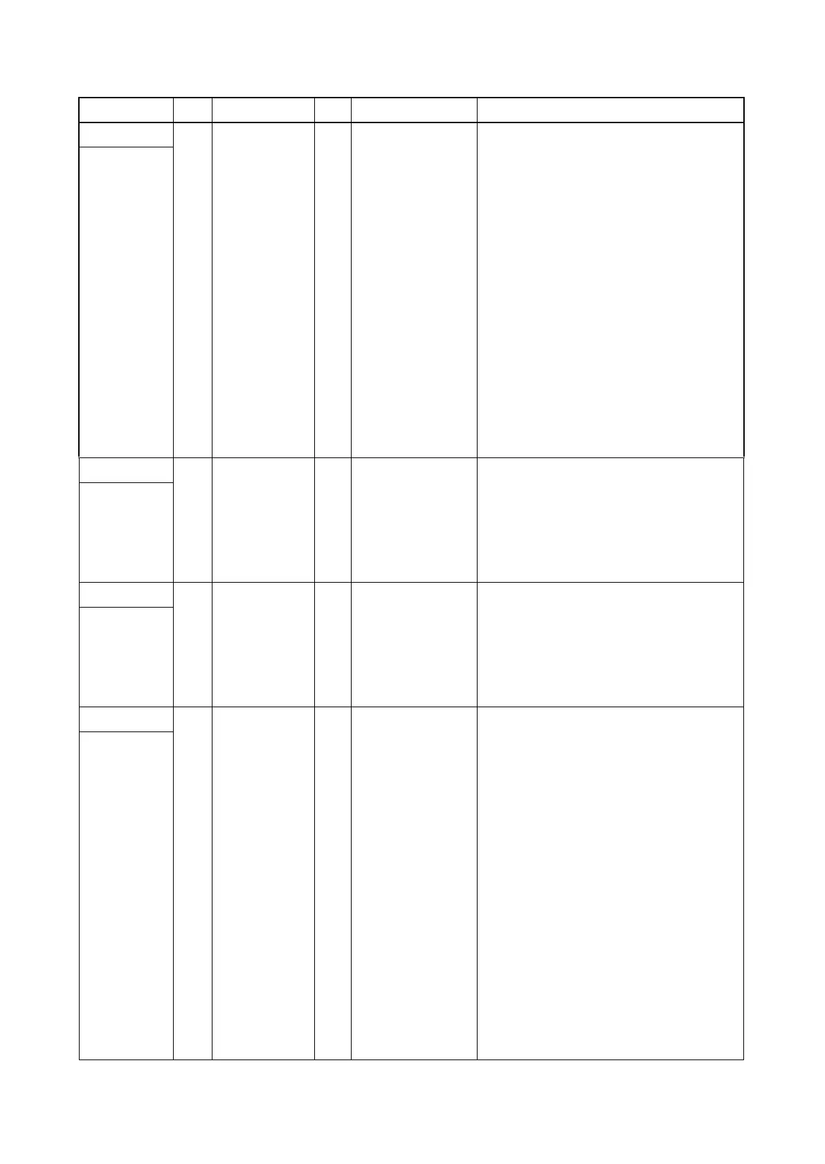
Connector Pin Signal I/O Voltage Description
YC2 1 DAT3 I/O DC0V/3.3V Control signal
Connected to
the SD card
I/F
2 CMD I/O DC0V/3.3V Command control signal
3 VSS - - Ground
4 VDD O DC3.3V Control signal
5 CLK O DC0V/3.3V 3.3 V DC power output
6 VSS - - Ground
7 DAT0 I/O DC0V/3.3V Data bus signal
8 DAT1 I/O DC0V/3.3V Data bus signal
9 DAT2 I/O DC0V/3.3V Data bus signal
10 Delective_Car
d_Switch
I DC0V/3.3V Control signal
11 Common_Con
tact
- - Control signal
12 WPSwitch I DC0V/3.3V Control signal
YC4 1 VBUS I DC0V/5.0V 5 V DC power output to USB device
Connected to
the USB
Device
2 D- I/O Analog USB data signal
3 D+ I/O Analog USB data signal
4 GND - - Ground
YC6 1 VBUS O DC0V/5.0V 5 V DC power output to USB host
Connected to
the USB
HOST
2 D- I/O Analog USB data signal
3 D+ I/O Analog USB data signal
4 GND - - Ground
YC7 1 +5.0V1_C1 O DC5.0V 5 V DC power output to eKUIO
Connected to
the eKUIO
2 GND - - Ground
3 RESET O DC0V/3.3V Reset signal
4 +5.0V2_C O DC5.0V 5 V DC power output to eKUIO
5 GND - - Ground
6 IRQ I DC0V/3.3V Interrupt signal
7OPEN -- NC
8OPEN -- NC
9OPEN -- NC
10 OPEN - - NC
11 GND - - Ground
12 OPEN - - NC
 Loading...