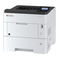
2T6/2T7/2T8/2T9
2-3-4
YC31 20 NINIT I DC0V/3.3V Reset signal
Connected to
the
IEEE1284
21 PDATECT I DC0V/3.3V OP detection signal
22 GND - - Ground
YC32 1 +24V0 I DC24V 24 V DC power input
Connected to
the engine
PWB
2 +24V0 I DC24V 24 V DC power input
3 +24V0 I DC24V 24 V DC power input
4 +3.3V0_PM O DC3.3V 3.3 V DC power output
5 +3.3V3_E O DC3.3V 3.3 V DC power output
6 +3.3V3_E O DC3.3V 3.3 V DC power output
7 +5.0V1_C1 O DC5.0V 5 V DC power output
8 +3.3V1_C O DC3.3V 3.3 V DC power output
9 DUTY_CONT
ROL
O DC0V/3.3V(pulse) PI / Sensor intermittent control signal
10 E2C_SDAT I DC0V/3.3V Serial communication data output
11 C2E_SDAT O DC0V/3.3V Serial communication data input
12 C2E_SCK O DC0V/3.3V Serial communication clock signal
13 E2C_SDIR I DC0V/3.3V Serial communication direction signal
14 E2C_SBSY I DC0V/3.3V System busy signal
15 GND - - Ground
16 VBUS_USBH
_3
O DC0V/5.0V 5 V DC power output to USB
17 GND - - Ground
18 USBH_DP3 I/O Analog USB differential data
19 USBH_DN3 I/O Analog USB differential data
20 GND - - Ground
21 SDIF_DAT0 I/O DC0V/3.3V WiFi input and output data
22 SDIF_DAT1 I/O DC0V/3.3V WiFi input and output data
23 SDIF_DAT2 I/O DC0V/3.3V WiFi input and output data
24 SDIF_DAT3 I/O DC0V/3.3V WiFi input and output data
25 SDIF_SDCLK O DC0V/3.3V WiFi input and output data
26 GND - - Ground
27 SH1D O DC0V/3.3V Sample-and-hold signal
28 GND - - Ground
29 LDOUT_1_DN O LVDS Video data
30 LDOUT_1_DP O LVDS Video data
31 GND - - Ground
32 GND - - Ground
Connector Pin Signal I/O Voltage Description
 Loading...