3 3
3 3
3
oo
oo
o
voltage must be between 12 and 16V.
➭
HIGH RAIL CHECK:HIGH RAIL CHECK:
HIGH RAIL CHECK:HIGH RAIL CHECK:
HIGH RAIL CHECK:
When the output signal (Positive half-wave) is less than 44Vp the voltage
on D2 cathode must remain constant at 50V, when the output signal
exceeds 44Vp the voltage must follow the output signal with 6V offset
(see
Fig.1 Trace B
), to check the negative high rail connect the probe to
D18 anode (see
Fig.1 Trace C
).
Connect the 4Ω 1000W load on the output and repeat the INITIAL and
HIGH RAIL checks.
Check the signal clipping, it must occur at 130±5Vpp (see
Fig.2 Trace
ABC
).
➭
SIGNAL/CLIP SENSOR CHECK:SIGNAL/CLIP SENSOR CHECK:
SIGNAL/CLIP SENSOR CHECK:SIGNAL/CLIP SENSOR CHECK:
SIGNAL/CLIP SENSOR CHECK:
Set the LEVEL pot to minimum, set the scope timebase at 1V/div. 200µS/
div., then increase the level and check the SIGNAL/CLIP led activity: it
must turn on (green light) when the amplifier output is higher than 5Vpp.
Set the scope at 50V/div. and increase the level, check the led: it must
change from green to red colour when the amplifier output signal clip.
➭
CURRENT AND SHORT CIRCUIT SENSOR CHECK:CURRENT AND SHORT CIRCUIT SENSOR CHECK:
CURRENT AND SHORT CIRCUIT SENSOR CHECK:CURRENT AND SHORT CIRCUIT SENSOR CHECK:
CURRENT AND SHORT CIRCUIT SENSOR CHECK:
Set the CH2 sensitivity to 0.5V/div., connect the scope CH1, GND clip at
CN6 (AMP output) and the probe tip at CN5 (GND terminal), CH2 probe
tip alternatively on TR6, TR11 (NPN) and TR16, TR22 (PNP) emitters.
Set the generator to have approx. 1Vp on the emitters: their difference
must be less than 10% one each other (see
Fig.3 Trace A
). The NPN or
PNP transistors out of tolerance must be replaced with a new selected
pair.
Connect a 2Ω 2000W load. Connect the CH1 probe tip on TR16 emitter
and the CH2 probe tip on TR11 emitter. Increase the input signal, the
output current limiter must keep the emitter voltages (both half channel) at
1.2Vp approx. (see
Fig.3 Trace B
).
Temporarily short the amplifier output: the current limiter must keep the
emitter voltages (both half channel) at 0.7Vp (see
Fig.3 Trace C
).
➭
COOLING FAN & PROTECTION CHECK:COOLING FAN & PROTECTION CHECK:
COOLING FAN & PROTECTION CHECK:COOLING FAN & PROTECTION CHECK:
COOLING FAN & PROTECTION CHECK:
Short circuit pins 11 and 12 of OC1 on Driver board, the fan must run at
max. speed (20÷23Vdc on its tips).
Short circuit pins 9 and 10 of OC1 on the same board, the PROTECT led
must turn on immediately, the fan must run at max. speed. The PROTECT
led of the other channel must also turn on after 2 Sec. and the relay must
disconnect the transformers from the mains.
Remove the short circuit, after 3 Sec. both PROTECT leds must turn off
and the relay must re-connect the transformers to the mains.
Temporarily short the emitter and the collector of TR7 (Driver board) the
PROTECT led must turn on and the relay must disconnect the transform-
ers from the mains.
Turn off the amplifier to reset it, wait a minute to let the supply caps
discharged.
➭
OFFSET SENSOR CHECK:OFFSET SENSOR CHECK:
OFFSET SENSOR CHECK:OFFSET SENSOR CHECK:
OFFSET SENSOR CHECK:
Set the Variac to zero voltage output, disconnect the amplifier load and
the supply connection to the Power board (CN1,2,7,8), turn on the ampli-
fier, connect temporarily (by means of a suitable conductor wire) CN6 to
+15Vdc, the PROTECT led must turn on immediately; the fan must run at
maximum speed).
Reset the protection turning off the amplifier, turn it on again, connect
temporarily (by means of a suitable conductor wire) CN6 to -15Vdc, the
led PROTECT must turn on again.
➭
SOA ADJUSTMENT:SOA ADJUSTMENT:
SOA ADJUSTMENT:SOA ADJUSTMENT:
SOA ADJUSTMENT:
Set the scope sensitivity at 5V/div. (both channels) and connect the CH1
probe on D12 cathode and the CH2 probe on D11 anode on Driver board,
check the voltage across D12 and D11 zener diodes: it must be
14.8±0.1V; increasing 10dB the generator level this voltage does not
decrease more than 0.5V.
Connect the 4Ω 1000W load, set the scope sensitivity at 2V/div. and
connect the CH1 probe tip at R43 side CN3 and the CH2 probe tip at R36
side CN2. Decrease the signal level until two sinusoid appear on the
scope as shown in
Fig 4 Trace AB
.
Their max. amplitude must be 5.5Vp (the outer) and 1.5Vp (the inner) as
shown in
Fig 5 Trace A,B
; increasing a bit the generator signal, the inner
sinusoid must produce spikes on its peaks as shown in
Fig 5 Trace A,B
.
Connect the 2Ω 1000W load, set the scope sensitivity at 1V/div. (both
channels) and connect its probes to the collectors of TR8 (CH1) and
TR11 (CH2) on Driver Board.
Disconnect the fan; wait until the temperature is 90°C (require some
minutes) then decrease the input to zero.
Adjust the trimmers R20 and R40, until the scope traces go respectively
at -2.2Vdc and +2.3Vdc; turn on the cooling fan and wait until the tem-
perature goes down to 80°C; then turn it off.
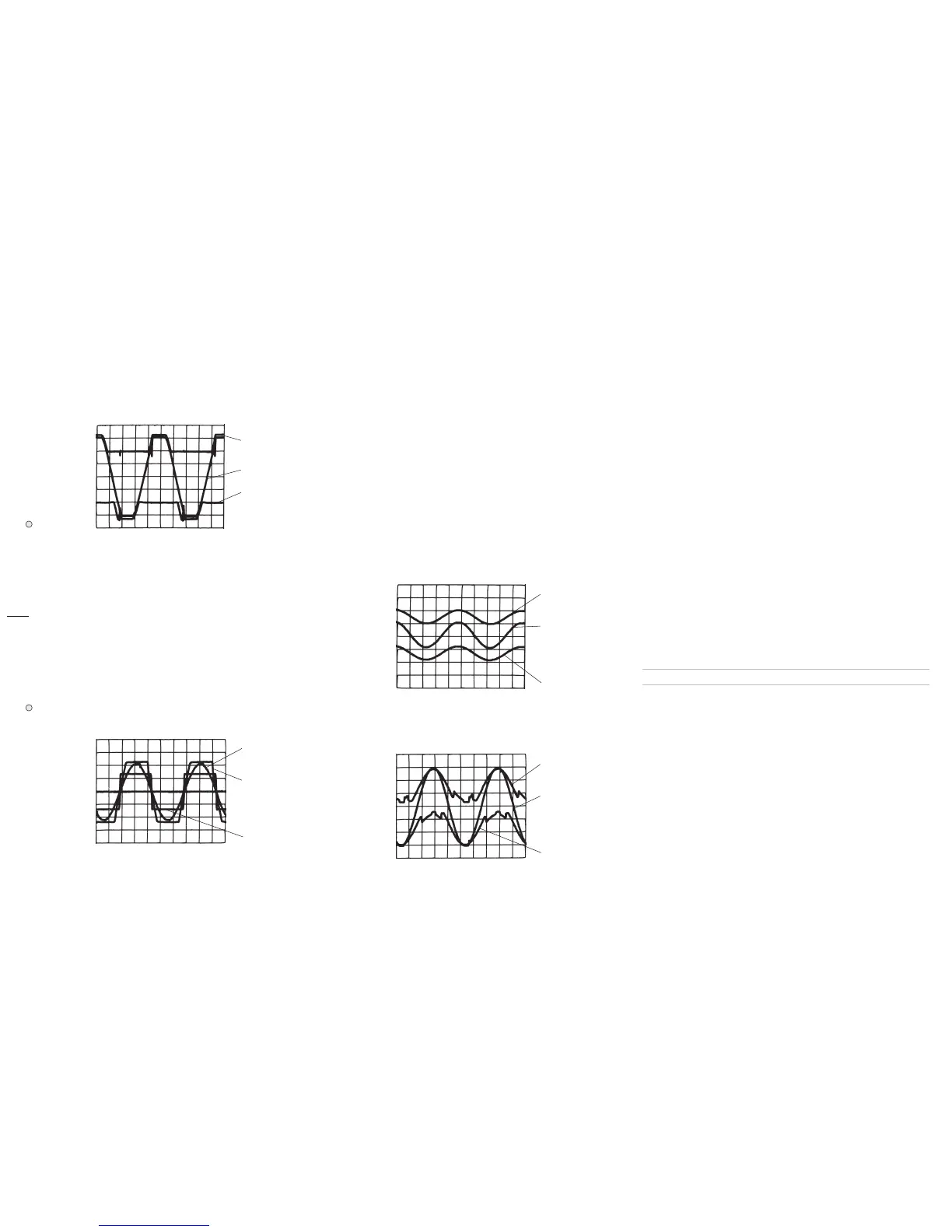
Fig. 2Fig. 2
Fig. 2Fig. 2
Fig. 2
Fig. 3Fig. 3
Fig. 3Fig. 3
Fig. 3
Trace A (0.5V/div.)
Trace B (0.5V/div.)
Trace C (0.5V/div.)
Fig. 5Fig. 5
Fig. 5Fig. 5
Fig. 5
Trace A (2V/div.)
Trace C (20V/div.)
(Amplifier Output)
Trace B (2V/div.)
Fig. 4Fig. 4
Fig. 4Fig. 4
Fig. 4
Trace A (2V/div.)
Trace C (20V/div.)
(Amplifier Output)
Trace B (2V/div.)
Reconnect the 4Ω 1000W load, adjust the level for the maximum dis-
placement of the scope tracks toward the centre of the scope screen (-
3dB approx.); the SOA control circuit (Protect led light on) will start at
90±2°C.
Reconnect the cooling fan and check with the Multimeter its supply volt-
age: it must be 20V or more (max speed).
At 70°C heatsink temperature, short circuit the amplifier output and check
the scope traces: they must displace 1V toward the centre of the screen,
respect to the previous position with 4Ω load.
Remove the short and decrease the input level to zero. The temperature
will decrease: at 65..75°C the speed of the cooling fan must change from
max to min speed. In case of a fan misbehaviour try to replace the D10
zener diode: if speed change at 75°C or more replace with a lower volt-
age zener diode, if speed change at 60°C or less replace with a higher
voltage zener diode.
➭
BIAS ADJUSTMENT:BIAS ADJUSTMENT:
BIAS ADJUSTMENT:BIAS ADJUSTMENT:
BIAS ADJUSTMENT:
Connect the Multimeter across
R54 of Power board, when the heatsink
temperature rises at 50°C, turn off the cooling fan and adjust R31 to read
2mV.
Set the scope sensitivity at 1V/div.(CH1), and connect the GND clip to the
amplifier GND (CN5) and the probe tip on the output (CN6). Adjust the
generator level until the sinewave appears at full screen amplitude, No
crossover distortion must be detectable: if necessary re-adjust R31. Re-
connect the fan.
➭
BANDWIDTH CHECK:BANDWIDTH CHECK:
BANDWIDTH CHECK:BANDWIDTH CHECK:
BANDWIDTH CHECK:
Sweep the generator frequency from 20Hz to 20KHz, the output level
must have not detectable level changes.
➭
SLEW RATE CHECK:SLEW RATE CHECK:
SLEW RATE CHECK:SLEW RATE CHECK:
SLEW RATE CHECK:
Set the scope sensitivity to 10V/div. 1mS/div. and set the generator to
1KHz square wave mode. Check the output square wave rising and falling
edge slopes: both must be 12V/µS or more.
➭ Disconnect the Variac and re-connect the transformer primaries to the
PROTECTIONS board (be careful to connect the two transformers out of
phase).
Inputs Board CheckInputs Board Check
Inputs Board CheckInputs Board Check
Inputs Board Check
➭ These procedures are intended for one channel at a time, repeat these
operations for the other channel.
➭
SETUP:SETUP:
SETUP:SETUP:
SETUP:
Connect the CH1 probe to amplifier input of the channel under test and
set both at 500mV/div. 200mS/div.
Connect the CH2 probe to amplifier output of the channel under test and
set it at 10mV/div. 200mS/div.
Set the audio generator at 1KHz sinus. 775mV
RMS
(0dB).
Set the LEVEL potentiometers full clockwise.
The load resistor is disconnected.
➭
CMRR ADJUSTMENTCMRR ADJUSTMENT
CMRR ADJUSTMENTCMRR ADJUSTMENT
CMRR ADJUSTMENT
Temporarily disconnect pin 3 from pin 1and short the pin 2 (positive input)
and pin 3 (negative input) of XLR input socket.
Adjust the trimmer R10 (channel A) or R21 (channel B) to obtain the
minimum output level.
➭
GAIN ADJUSTMENTGAIN ADJUSTMENT
GAIN ADJUSTMENTGAIN ADJUSTMENT
GAIN ADJUSTMENT
Re-set the input signal at pin 2 (positive input) and pin 3 (negative input)
short with pin 1 (GND) of XLR input socket
Set CH2 scope at 500mV/div. and connect it to the output of INPUTS
board (CN3 pin9 for channel A or CN3 pin7 for channel B).
Set the input SENSITIVITY (SW1) at 2.25Vrms, adjust the trimmer R5
Trace B (20V/div.)
Trace A (20V/div.)
Trace C (20V/div.)
 Loading...