- 7 -
LGE Internal Use OnlyCopyright©2008 LG Electronics. Inc. All right reserved.
Only for training and service purposes
6. Component input ADC
6-1
. Component Gain/Offset Adjustment
(1)
Convert to PC in Input-source(refer to I2C command at page 10)
(2) Signal equipment displays
1) Impress Resolution 480i
Model : 209 in pattern Generator(480i Mode)
Pattern : 65 in pattern Generator(MSPG-925 Series)
2) Impress Resolution 1080i
Model : 223 in pattern Generator(1080i Mode)
Pattern : 65 in pattern Generator(MSPG-925 Series)
6-2. Confirmation
(1) We confirm whether “0xB3(480i)/0xBC(1080i)” address
of EEPROM “0xA2” is “0xAA” or not.
(2) If “0xB3(480i)/0xBC(1080i)” address of EEPROM “0xA2”
isn’t “0xAA”, we adjust once more.
(3) We can confirm the ADC values from
“0xAD~0xB2(480i)/0xB6~BB(1080i)” address in a page
“0xA2”.
* Manual ADC process using Service Remocon. After enter
Service Mode by pushing “ADJ” key, execute “ADC Adjust”
by pushing “
G“ key at “ADC CALIBRATION : RGB-C”.
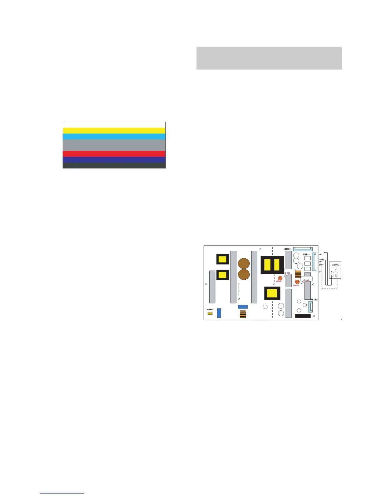
7. POWER PCB Assy Voltage
Adjustments (Va, Vs Voltage adjustments)
7-1. Test Equipment : D.M.M. 1EA
7-2.Connection Diagram for Measuring
: refer to Fig.3
7-3. Adjustment Method
(1) Va Adjustment
1) After receiving 100% Full White Pattern, HEAT RUN.
2) Connect + terminal of D.M.M to Va pin of P811, connect
- terminal to GND pin of P811.
3) After turning VR901, voltage of D.M.M adjustment as
same as Va voltage which on label of panel right/top.
(Deviation; ±0.5V)
(2) Vs Adjustment
1) Input signal : RF noise signal.
2) Connect + terminal of D.M.M to Vs pin of P811, connect
– terminal to GND pin of P811.
3) After turning VR951, voltage of D.M.M adjustment as
same as Va voltage which on label of panel right/top.
(Deviation; ±0.5V)
Each PCB assembly must be checked by check JIG set.
(Because power PCB Assembly damages to PDP Module,
especially be careful)
(Fig.2)
(Fig.3) Connection diagram of power adjustment for measuring

 Loading...