LG
November 2017
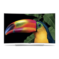
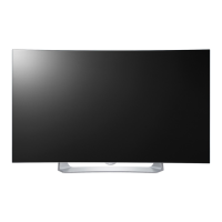
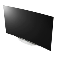
55EG9600 (2015 OLED) Power Supply
Power Supply Operation Explained (1 of 2)
Page 04
(1) When AC is applied to the AC Filter the AC is filtered to prevent Switching noise from the Power Supply radiating back out into the AC Power
lines. This filtered AC is then output P102 to the Power Supply (SMPS) P102. During Standby, the SMPS outputs 3.5V_ST (3.56V) via P201,
24pin connector pins 5, 7 and 8 to the Main board P2399. It then goes through coil L2395 and is filtered by C2395. Note, this line is now Labeled
+3.5V_ST. The output 3.5V_ST is routed to the Microprocessor IC3000 pin 48 as its main power source. It also goes to the Reset circuit R3030,
C3004. At the moment 3.5V arrives at C3004 (+) side, the capacitor isn’t charged, so pin 40 of the Micro is low while the power input pin 48 is
high. This is known as the reset state, where the Microprocessor is reset to the first operational state. As C3004 charges through R3030, pin 40
pulls up and the Micro comes out of Reset. The TV is now in the Stand-By state.
The 3.5V_ST is also routed to pull-up resistors to the Key 1 and 2 lines pulling them up to 3.54V. It is also sent to the IR receiver and as source
voltage for the Power on switch Q2502, but it is not on at this time.
(2) The 3.5V_ST line is also routed to Q3001 CEC buffer, IC4100 +3.5V_WIFI regulator (in case “LG Connect Apps” is turned on, IC6801 RS-232C
Buffer, IC201 +3.5V_WOL regulator (to activate WiFi processing during Standby if “LG Connect Apps is turned on, IC2307 Power Det IC. It is
also pull-up voltage for Q2398 RL_ON driver, Q2303 DCP_CTRL Driver, for the Key 1 and 2 lines, IR and the Room light sensor data lines EYE
SDA/SCL. It is also Power for the IR/Joystick Board P4100 pin 4.
(3) When the Power on is pressed on the Joy Stick (Press in and hold), the Key2 line of P4101 drops to 0.58V so pin 32 of the Micro drops. This
notifies the Micro that the TV should turn on. If the Power On key on the Customer’s Remote is pressed, The IR receiver sends this signal
(3.76V p/p) to the Microprocessor pin 6 and the TV knows by this signal to turn on.
(4) The Micro outputs a low on pin 36 (RL_ON) which is routed through R2389 to pin 2 of Q2398 turning it on. The +3.5V_ST on pin 1 is then
switched out pin 3 and on to the SMPS via pin 1 of P2399. This high arrives at P201 pin 1 and on to the Controller on the SMPS. This command
turns on the 12VM and the 24VS (which is sent back to the Main). 12VM (Main) for all Video /Audio processing and 24VS for (Sound).
(5) The 12VM (11.99V) and the 24VS (24.59) lines are routed out P201 (12VM pins 11-15 and 24VS pins 19-22) and on to the Main board P2399.
The 24VS (labeled +24V on schematic) is used for the Audio amplifier IC5800 (Main).
The 12VM (Labeled +12V) is routed to many different regulators, but for this “Power On” circuit discussion it goes through two coils L2396 and
L2397 and on to the different regulators.
(6) When the 12VM (+12V) is routed to IC2307 (Power Detector pin 3). The +24V is also monitored by IC2308 and tied to the same POWER_DET
Line. These ICs then outputs a high (POWER_DET) to the Micro pin 14 to notify the Micro that the 12V and 24V voltage has arrived. So the
Micro can continue turning on the rest of the set. If missing, the TV will click on and then Click off. This fault shows up in the Power Off Status as
“5VMNT”.
(7) Once the Micro knows the 12VM and 24VS has arrived, it outputs a high on pin 33 (Power_ON/OFF2_1) which is routed through R2303 to pin 1
of IC2302 turning it on. This IC is the +3.3V_NORMAL regulator. The 3.3V output is routed to many different circuits, but one of them is as a
pull-up voltage through R2394 to the INV_CTL (DRV_ON) line. However, the Micro is holding down INV_CTL P2399 pin 2 at this time.

 Loading...