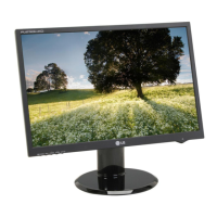
Do you have a question about the LG Flatron L226WTQ and is the answer not in the manual?
Details on LCD panel properties, viewing angles, luminance, and contrast.
Information on signal inputs, maximum resolution, and power requirements.
Environmental operating conditions and physical dimensions/weight.
Details the pinout for the DVI-D digital connector.
Highlights critical safety components and modification risks.
Provides guidelines for safely handling the LCD module.
Lists essential precautions before and during servicing.
Explains how to prevent damage from static electricity.
Step-by-step guide for removing and installing ICs.
Procedures for replacing small-signal and power transistors.
Steps for replacing diodes, fuses, and resistors.
Method for repairing foil traces connected to IC pins.
Method for repairing foil traces at non-IC connections.
Instructions for removing screws during disassembly.
Procedure for detaching the front cover.
Steps for removing the printed circuit boards.
Instructions for removing the back cover.
Explanation of the video controller's functions and components.
Details the power supply and inverter circuit functions.
Describes the microcontroller unit and its associated components.
Steps for setting up the user port for EDID operations.
Instructions for reading and writing EDID information using WinEDID.
Functions for initializing and automatically balancing color.
Options for selecting aging mode and initializing EEPROM.
Manually adjusting RGB gain and offset values.
Steps to diagnose and fix power-related problems.
Troubleshooting steps for no raster on the LIPS board.
Troubleshooting steps for no raster on the main board.
Steps to diagnose and resolve DPM (Digital Panel Manager) problems.
Detailed list of parts with their part numbers and descriptions.
Part numbers for accessories and capacitors.
Part numbers for diodes, resistors, ICs, filters, and transistors.
Part numbers for connectors, switches, and other components.
Diagram showing the component layout on the top side of the main PCB.
Diagram showing the component layout on the bottom side of the main PCB.
Schematic diagram for the LED Printed Circuit Board.
Illustration of button placement and functions.
Detailed circuit schematics for the scaler IC and related components.
Schematics for the power supply and wafer connections.
Circuit diagram for the control and button interface.
 Loading...