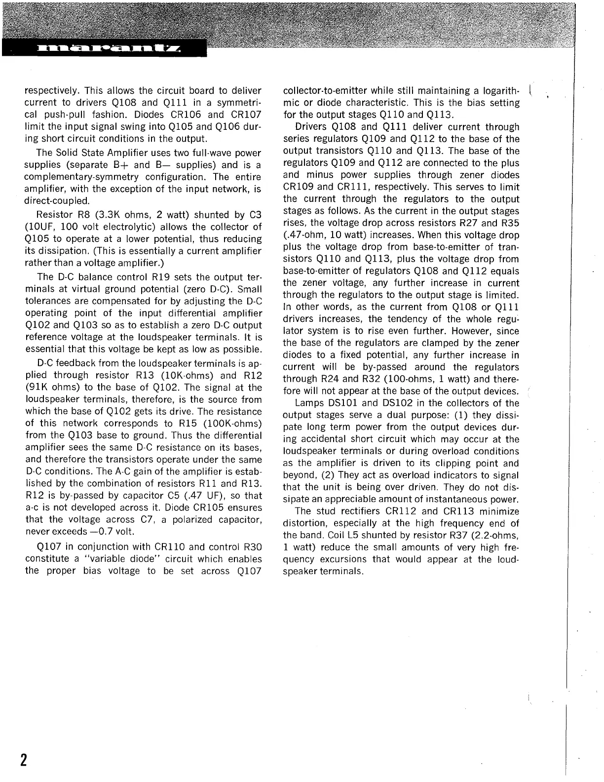
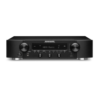
respectively. This allows the circuit board to deliver
current to drivers Q108 and
Qll
1
in
a symmetri-
cal push-pull fashion. Diodes CR106 and CR107
limit
the input signal swing into Q105 and Q106 dur-
ing short
circuit
conditions
in
the output.
The Solid State Amplifier uses two full-wave power
supplies (separate
B+
and
8-
supplies) and is a
complementary-symmetry configuration. The entire
amplifier, with the exception
of
the input network, is
direct-coupled.
Resistor
R8
(3.3K ohms, 2 watt) shunted
by
C3
(lOUF,
100
volt electrolytic) allows the collector
of
Q105 to operate at a lower potential, thus reducing
its dissipation. (This is essentially a current amplifier
rather than a voltage amplifier.)
The
D-C
balance control R19 sets the output ter-
minals at virtual ground potential (zero D-C). Small
tolerances are compensated
for
by adjusting the
D-C
operating point of the input differential amplifier
Ql02
and Q103
so
as
to establish a zero
D-C
output
reference voltage at the loudspeaker terminals.
It
is
essential
that
this voltage
be
kept
as
low
as
possible.
D-C
feedback from the loudspeaker terminals
is
ap-
plied through resistor R13
(l0K-ohms)
and R12
(91K ohms) to the
base
of
Q102. The signal at the
loudspeaker terminals, therefore,
is
the source from
which the base of
Ql02
gets its drive. The resistance
of
this
network corresponds to R15 (lO0K-ohms)
from the
Ql03
base to ground. Thus the differential
amplifier
sees
the same
D-C
resistance
on
its bases,
and therefore the transistors operate under the same
D-C
conditions. The
A-C
gain of the amplifier is estab-
lished
by
the combination of resistors
Rll
and
Rl3.
Rl2
is by-passed by capacitor
C5
(.47 UF),
so
that
a-c
is not developed across it. Diode CR105 ensures
that the voltage across
C7,
a polarized capacitor,
never exceeds
-0.
7 volt.
Q107
in
conjunction with
CRll0
and control R30
constitute a "variable
diode"
circuit which enables
the proper bias voltage to
be
set across Q107
2
collector-to-emitter while still maintaining a logarith-
mic
or
diode characteristic. This is the bias setting
for
the output stages
Qll0
and
Ql13.
Drivers Q108 and
Ql
11
deliver current through
series regulators Q109 and Q112 to the base
of
the
output transistors
Qll0
and Q113. The base
of
the
regulators Q109 and
Ql
12
are connected to the plus
and minus power supplies through zener diodes
CR109 and
CRlll,
respectively. This serves to
limit
the current through the regulators to the output
stages
as
follows.
As
the current
in
the output stages
rises, the voltage drop across resistors R27 and R35
(.47-ohm, 10 watt) increases.
When
this voltage drop
plus the voltage drop from base-to-emitter of tran-
sistors
Qll0
and Q113, plus the voltage drop from
base-to-emitter of regulators Q108 and
Ql
12 equals
the zener voltage, any
further
increase in current
through the regulators to the output stage is limited.
In
other words,
as
the current from Q108 or
Ql
11
drivers increases, the tendency
of
the whole regu-
lator system is to rise
even
further. However, since
the
base
of the regulators are clamped by the zener
diodes to a fixed potential, any
further
increase
in
current will
be
by-passed around the regulators
through R24 and R32 (100-ohms, 1 watt) and there-
fore will not appear at the base of the output devices.
Lamps DS101 and DS102
in
the collectors of the
output stages serve a dual purpose: (1) they dissi-
pate long term power from the output devices dur-
ing accidental short
circuit
which may occur at the
loudspeaker terminals
or
during overload conditions
as
the amplifier is driven to its clipping point and
beyond, (2) They act
as
overload indicators to signal
that the unit is being over driven. They do not dis-
sipate
an
appreciable amount of instantaneous power.
The stud rectifiers CR112 and
CRl
13 minimize
distortion, especially at the high frequency end of
the band. Coil
L5
shunted by resistor R37 (2.2-ohms,
1 watt) reduce the small amounts of very high fre-
quency excursions that would appear at the loud-
speaker terminals.