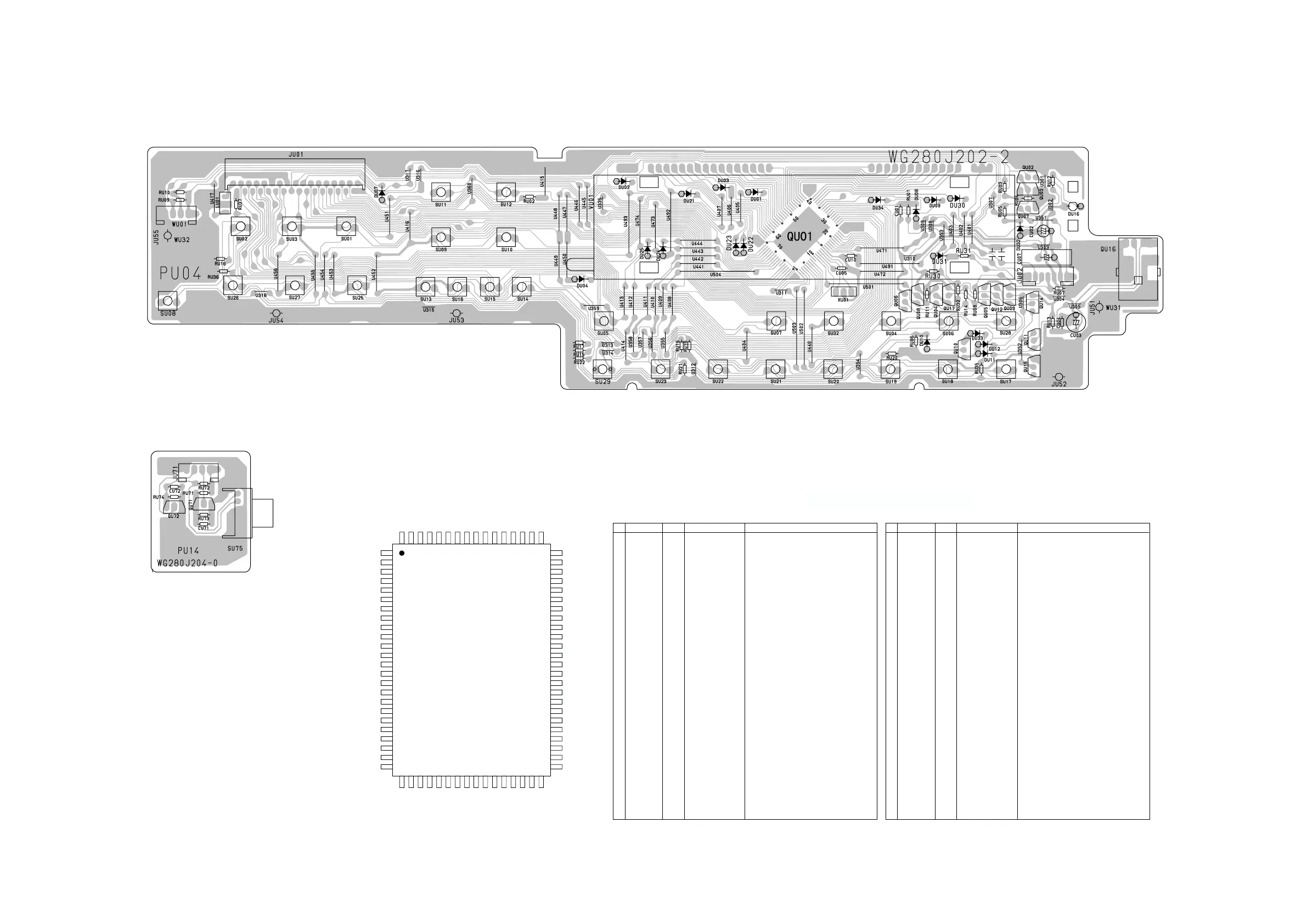
PU04 Display and Key Input P.C. Board
QU01 QU06
QU08
QU04
QU17
QU10
QU05
QU12 QU09
QU02
QU03
QU07
QU14
QU11
QU15
QU16
QU72 QU71
PU14 Rotary Encorder P.C. Board
QU01:TMP87CP71F
1
2
3
4
5
6
7
8
9
10
11
12
13
14
15
16
17
18
19
20
21
22
23
24
25 26 27 28 29 30 31 32 33 34 35 36 37 38 39 40
80 79 78 77 76 75 74 73 72 71 70 69 68 67 66 65
64
63
62
61
60
59
58
57
56
55
54
53
52
51
50
49
48
47
46
45
44
43
42
41
RU:Pull UP,USE:Using Port type,act.:active level,OPT:Option
RST:port setting when Reset start,STOP:port setting when STOP mode
No Port Name Use Sig.Name Description
1 P10/INT0 I Request (I2C Request)
2 P11/INT1 I Head Phone Head Phone SW input
3 P12/INT2 INT MAIN RC-5 Main RC-5 input
4 P13/DVO I POWER DET. Power Detect input
5 P14 I OSD SYNC0 OSD Sync.input
6 P15/TC2 I OSD SYNC1 OSD Sync.For S input
7 P16 I Pulse Enc.A for Master Volume
8 P17 I Pulse Enc.B for Master Volume
9 TEST to GND
10 P21/XTIN O POWER OFF Power Off output
11
P22/XTOUT
O SURR.RST Surr.module Reset
12 RESET
13 XIN Fc=8.00MHz in
14 XOUT Fc=8.00MHz out
15 Vss
16 P20/STOP STOP Power Down used STOPinput
17 P30/INT3 INT MULTI RC-5 Multi Room RC-5 in
18 P31/TC4 I/O SURR.ACK Surr.module interface
19 P32/SCK SCK SURR.CLK Surr.module interface
20 P33/SI SI SURR.DI Surr.module interface
21 P34/SO SO SURR.DO Surr.module interface
22 P35/HSCK HSCK OSD CLK OSD IC interface
23 P36 I/O SURR.REQ Surr.module interface
24 P37/HSO HSO OSD DO OSD IC interface
25 P00 O OSD CE0 OSD IC interface
26 P01 O OSD CE1 OSD IC interface for S
27 P02 O CE3 for 4094 interface
28 P03 O CE2 for TUNER,etc..
29 P04 O CE1 for Volume
30 P05 O CE0 for Analog SW
31 P06 O SCLK SO interface
32 P07 O SDATA SO interface
33 Vdd
34 P60/G15 O PAL/NTSC OSD mode output
35 P61/G14 O KILL IR Kill IR for RC-5 output
36 P62/G13 O KILL Video Kill Video Signal
37 P63/G12 O DIGTAL SEL. (added switch)
38 P64/G11 G FTD G12 FTD Grid output
39 P65/G10 G FTD G11 FTD Grid output
40 P66/G9 G FTD G10 FTD Grid output
41 P67/G8 G FTD G9 FTD Grid output
42 P70/G7 G FTD G8 FTD Grid output
43 P71/G6 G FTD G7 FTD Grid output
44 P72/G5 G FTD G6 FTD Grid output
45 P73/G4 G FTD G5 FTD Grid output
46 P74/G3 G FTD G4 FTD Grid output
47 P75/G2 G FTD G3 FTD Grid output
48 P76/G1 G FTD G2 FTD Grid output
49 P77/G0 G FTD G1 FTD Grid output
50 P80/S0 S FTD S1 FTD Segment output
51 P81/S1 S FTD S2 FTD Segment output
52 P82/S2 S FTD S3 FTD Segment output
53 P83/S3 S FTD S4 FTD Segment output
54 P84/S4 S FTD S5 FTD Segment output
55 P85/S5 S FTD S6 FTD Segment output
56 P86/S6 S FTD S7 FTD Segment output
57 P87/S7 S FTD S8 FTD Segment output
58 P90/S8 S FTD S9 FTD Segment output
59 P91/S9 S FTD S10 FTD Segment output
60 P92/S10 S FTD S11 FTD Segment output
61 P93/S11 S FTD S12 FTD Segment output
62 P94/S12 S FTD S13 FTD Segment output
63 P95/S13 S FTD S14 FTD Segment output
64 P96/S14 S FTD S15 FTD Segment output
65 P95/S15 S FTD S16 FTD Segment output
66 Vkk FTD Power Supply
67 P40/KEY0 KEY Key in 0 Key Matrix input
68 P41/KEY1 KEY Key in 1 Key Matrix input
69 P42/KEY2 KEY Key in 2 Key Matrix input
70 P43/KEY3 KEY Key in 3 Key Matrix input
71 P44/KEY4 KEY Key in 4 Key Matrix input
72 P45/KEY5 KEY Key in 5 Key Matrix input
73 P46/KEY6 KEY Key in 6 Key Matrix input
74 P47/KEY7 KEY Key in 7 Key Matrix input
75 P50/CIN3 O RC-5 out RC-5 output
76 P51/CIN2 I/O I2C SCL (I2C SCL)
77 P52/CIN1 I/O I2C SDA (I2C SDA)
78 P53/CIN0 CIN S.STRENGTH Signal Strength(A/D)
79 P54 I TUNER SD SD input
80 P55/PWM I TUNER DO DO input
No Port Name Use Sig.Name Description
21 22