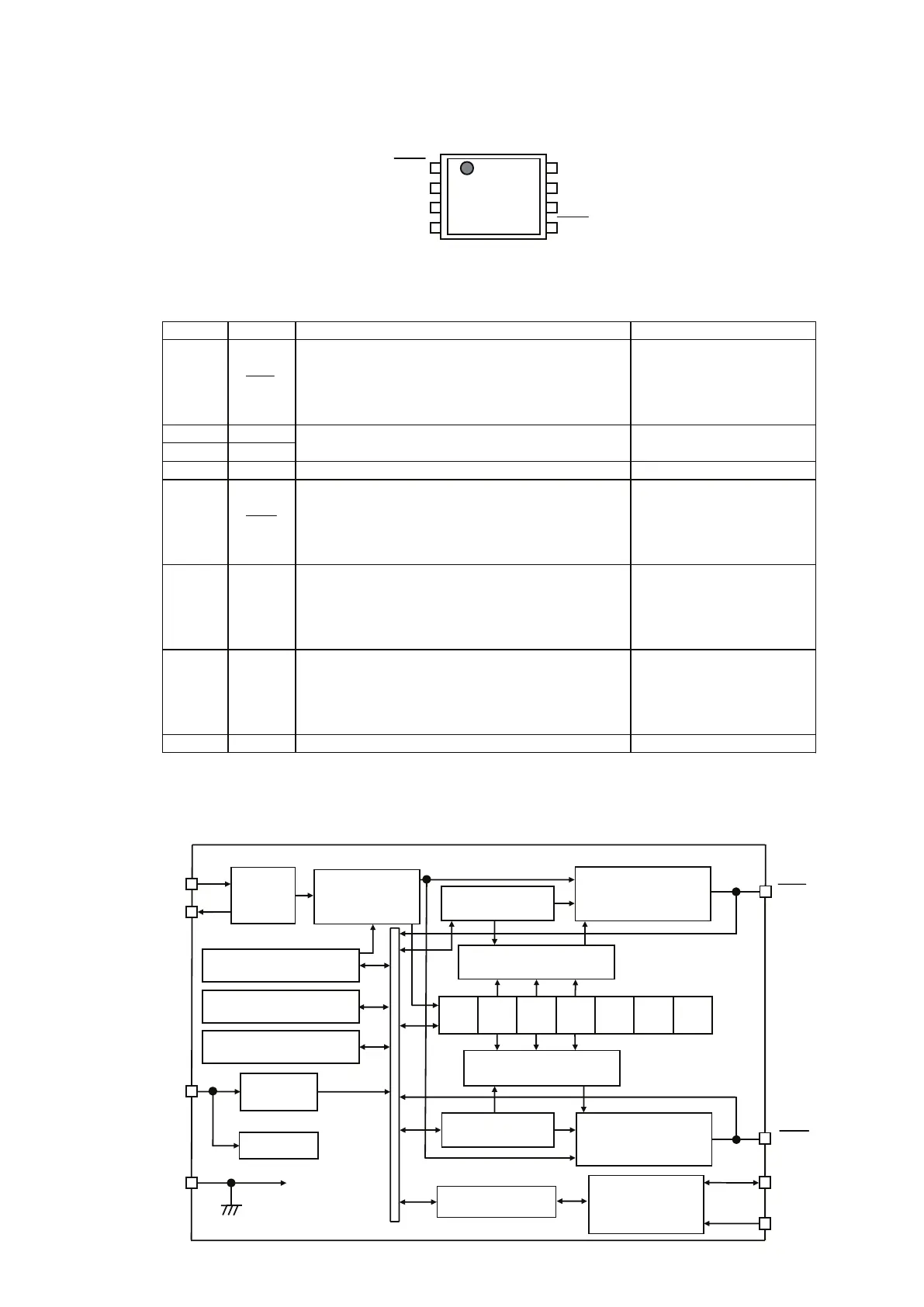
45
Q311 : S-35390A-I8T1G
1
2
3
4
8
7
6
5
VDD
SDA
SCL
INT2
INT1
XOUT
XIN
VSS
SNT-8A (TOP VIEW)
Pin No. Symbol Description Configuration
1
INT1
Interrupt 1 signal output pin
Depending on the mode set by INT1 register_1
and the status register, it outputs low or a clock
when the time is reached. It is disabled by
rewriting the status register.
Nch open-drain output (no
protective diode on the side
of VDD)
2 XOUT Crystal oscillator connect pin (32,768 Hz)
⎯
3 XIN
(C
d
built in, C
g
external)
4 VSS Negative power supply pin (GND)
⎯
5
INT2
Interrrupt 2 signal output pin
Depending on the mode set by INT1 register_2
and the status register, it outputs low or clock
when time is reached. It is disabled by rewriting
the status register.
Nch open-drain output (no
protective diode on the side
of VDD)
6 SCL
Serial clock input pin
Since signal processing is done on the SCL
signal rising/falling edge, give great care to the
rising/falling time and comply strictly with the
specifications.
CMOS input (no protective
diode on the side of VDD)
7 SDA
Serial data I/O pin
Normally, it is pulled up to the V
DD
voltage by a
resistor and connected with another open-drain
output or open-collector output device via a
wired-OR connection.
Nch open-drain output (no
protective diode on the side
of VDD)
CMOS input
8 VDD Positive power supply pin
⎯
PIN DESCRIPTION
Realtime data register
Status register_1
Oscillator
SCL
SDA
Power supply
voltage
detector
VDD
VSS
Comparator 1
Second Minute Hour
Day of
week
Day Month Ye a r
Shift register
Serial interface
INT1
XIN
XOUT
INT2
Comparator 2
Clock adjustment register
INT1 controller
Division, timing
generator
INT2 controller
Constant
voltage circuit
Status register_2
INT1 register_1
INT1 register_2
BLOCK DIAGRAM
 Loading...