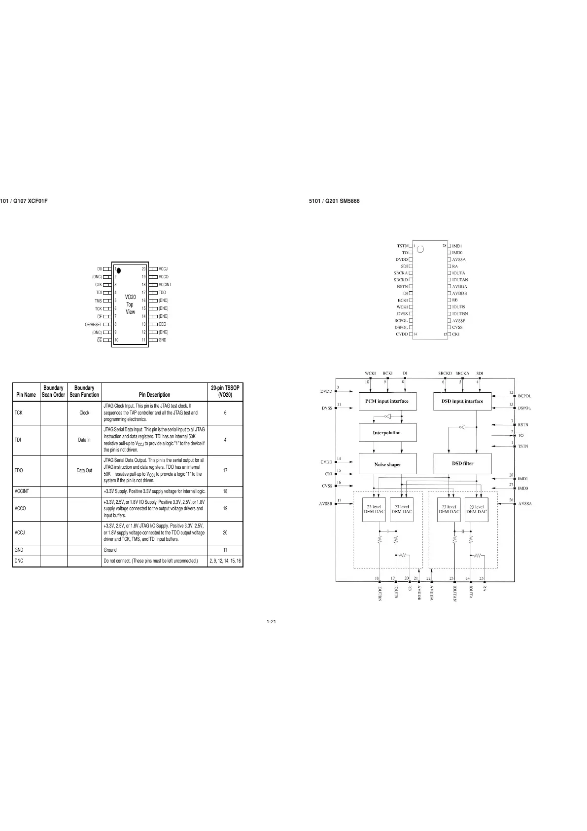
TCK
Clock
JTAG Clock Input. This pin is the JTAG test clock. It
sequences the TAP controller and all the JTAG test and
programming electronics.
6
TDI
Data In
JTAG Serial Data Input. This pin is the serial input to all JTAG
instruction and data registers. TDI has an internal 50K
resistive pull-up to V
CCJ
to provide a logic "1" to the device if
the pin is not driven.
4
TDO
Data Out
JTAG Serial Data Output. This pin is the serial output for all
JTAG instruction and data registers. TDO has an internal
50K resistive pull-up to V
CCJ
to provide a logic "1" to the
system if the pin is not driven.
17
VCCINT +3.3V Supply. Positive 3.3V supply voltage for internal logic.
18
VCCO
+3.3V, 2.5V, or 1.8V I/O Supply. Positive 3.3V, 2.5V, or 1.8V
supply voltage connected to the output voltage drivers and
input buffers.
19
VCCJ
+3.3V, 2.5V, or 1.8V JTAG I/O Supply. Positive 3.3V, 2.5V,
or 1.8V supply voltage connected to the TDO output voltage
driver and TCK, TMS, and TDI input buffers.
20
GND Ground
11
DNC Do not connect. (These pins must be left unconnected.) 2, 9, 12, 14, 15, 16
Pin Name
Boundary
Scan Order
Boundary
Scan Function Pin Description
20-pin TSSOP
(VO20)
VO20
Top
View
1
2
3
4
5
6
7
8
9
10
20
19
18
17
16
15
14
13
12
11
D0
(DNC)
CLK
TDI
TMS
TCK
CF
OE/RESET
(DNC)
CE
VCCJ
VCCO
VCCINT
TDO
(DNC)
(DNC)
CEO
(DNC)
GND
(DNC)
 Loading...