51 52
QK01 : AK4528
No. Pin Name I/O Function
1VCOM O
Common Voltage Output Pin, VA /2
Bias voltage of ADC inputs and DA C outputs.
2 AINR+ I Rch Positive Inp ut Pin
3 AINR- I Rch Negative Input Pin
4 AINL + I Lch Positive Inp ut Pin
5 AINL - I Lch Negative Inp ut Pin
6VREF I
Voltage Reference Input Pin, VA
Used as a voltage reference by ADC & DA C. VREF is connected externally to
filtered VA .
7 AGND - Analog Ground Pin
8 VA - Analog Power Supply Pin, 4.75
~
5.25V
9P/S I
Parallel/Serial Mode Select P in
ì Lî: Serial Mode, ì Hî: P arallel Mode
10 MC LK I Master Clock Input Pin
11 LRCK I Input/Output Channel Clo ck Pin
12 BICK I Audio Serial Data Clock Pin
13 SDTO O Audio Serial Data Output Pin
14 SDTI I Audio Serial Data Input Pin
CDTI I Control Data Input Pin in Serial Mode
15
CKS0 I Master Clock Select Pin
CCLK I Control Data Clock Pin in Serial Mo de
16
CKS1 I Master Clock Select Pin
CSN I Chip Select Pin in Serial Mode
17
DIF I
Digital A udio In terface Select Pin
ì Lî: 24bit MSB justified, ì Hî: I
2
S compatible
18 DFS I Double Speed Sampling Mo de Pin
19 PD N I
Power-Down Mode Pin
ì Hî: P ower up, ì Lî: P ower down reset and initialize the co ntrol register.
20 DEM0 I De-emphasis Control Pin
21 DEM1 I De-emphasis Control Pin
22 VT - Output Buffer Power Supply Pin, 2.7
~
5.25V
23 VD - Digital Power Supply Pin, 4.75
~
5.25V
24 DGND - Digital Grou nd Pin
25 AOUT L- O Lch Negative Analog Output Pin
26 AOUT L+ O Lch Positive A nalog Output Pin
27 AOUT R- O Rch Negative Analog Output Pin
28 AOUT R+ O Rch Positive A nalog Output Pin
Note: All input pins should not be left floating.
Left/Right
Left/Right Surround
Xtal
Center/Subwoofer
S/PDIF
Input
Data/
Control
A
E
F
Address
Test
Control
General Purpose
I/O Ports
Host
Parallel
Port
Serial
Output
Ports
Serial
Input
Ports
B
C
D
Figure 5. ZR38601 Simplified Block Diagram
4
16
20
Serial Host
SPI or Z2C
Interface
Internal Program/
Data ROM
20k x 32
Internal Program/
Data RAM
2k x 32
Internal
Data RAM
10k x 20
4
Serial Audio
Inputs
S/PDIF
Receiver
Parallel Host
Interface
Input Data
FIFO
8 x 9
S/PDIF
Transmitter
Serial Audio
Outputs
Memory
Interface
ICE
Interface
System
Oscillator &
DSP PLL
Audio PLL
GPIO
ZR38001
DSP Core
S/PDIF or
Left/Right Center
4
f
DSP
f
AUDIO
6
f
AUDIO
G
Timer
ZR38601 Signal Description Summary
Name Number Type
[1]
Description
Parallel Port (40)
A[19:0] 20 O Address bus of parallel port
D[19:15] 5 I/O Data bus of parallel port when selected for external memory (P/M
= 0)
D14/RDY 1 I/O or O Data bus (P/M = 0) or Ready output signal of parallel port when selected for parallel I/O (P/M = 1)
D13/ C/D 1 I/O or I Data bus (P/M = 0) or Command/Data select input of parallel port when selected for parallel I/O (P/M = 1)
D12/ERR 1 I/O or I Data bus (P/M = 0) or Error input signal of parallel port when selected for parallel I/O (P/M = 1)
D[11:4]/PP[7:0] 8 I/O Data bus of parallel port when selected for external memory (P/M
= 0) or Parallel Port I/O (P/M = 1)
CS 1 I/O Chip Select output for external memory or Chip Select input for parallel I/O
RD
1 I/O Read enable output for external memory or Read enable input for parallel I/O
WR 1 I/O Write enable output for external memory or Write enable input for parallel I/O
P/M 1 I Parallel I/O or Memory select for parallel port. Determined at time of RESET.
Serial Ports (13)
SPFRX 1 I S/PDIF Receiver input port
SDA, SDE, SDF 3 I Serial Data inputs. Ports A, E and F.
WSA/FSA 1 I/O Word Select or Frame Synchronization for input ports. An output when a master, an input when a slave.
SCKA 1 I/O Serial Clock for input ports. An output when a master, an input when a slave.
SDB 1 O Serial left and right Data output. Port B. Also, at RESET
defines SPI/Z2C for host serial interface.
SDC 1 O Serial left and right surround Data output. Port C. Also, at RESET defines Z2CADR[0] of Z2C address.
SDD 1 O Serial center and sub-woofer Data output. Port D. Also, at RESET
defines Z2CADR[1] of Z2C address.
SDG/SPFTX 1 O Serial Data output. Port G or S/PDIF Transmitter port. Also, at RESET defines the SCKP value.
WSB/FSB 1 I/O Word Select or Frame Synchronization for output ports. An output when a master, an input when a slave.
SCKB 1 I/O Serial Clock for output ports. An output when a master, an input when a slave.
SCKIN 1 I/O Serial master Clock output or master clock Input for output ports
General Purpose Ports (6)
MUTE
/GPIO5 1 I or I/O Mute input signal or can be programmed as General Purpose Input/Output 5
GPIO[4:2] 3 I/O Can be programmed as General Purpose Input/Output 4, 3 and 2
ERROR/GPIO1 1 O or I/O Error output signal or can be programmed as General Purpose Input/Output 1
DREQ
/GPIO0 1 O or I/O Data Request output signal or can be programmed as General Purpose Input/Output 0
Serial Host Interface (4)
SI 1 I Host Serial interface data Input. Also, at RESET defines Z2CADR[5] of Z2C address.
SO/SDA 1 I/O/T SPI host Serial interface data Output or Serial Data for Z2C
SCK/SCL 1 I SPI host Serial interface Clock input or Slave Clock input for Z2C
SS
1 I SPI host serial interface Slave Select input. Also, at RESET defines Z2CADR[4] of Z2C address.
ICE Interface (4)
TDI 1 I ICE Test interface Data Input
TDO 1 O/T ICE Test interface Data Output
TCK 1 I ICE Test interface Clock input
TMS 1 I ICE Test interface Mode Select
System Interface (7)
INT
1 I External Interrupt request input
RESET
1 I Reset input to start operation in known state
XTI 1 I External system clock Input or connection to external crystal, at frequency f
XTI
XTO 1 O Output connection to external crystal
CLKOUT 1 O Clock Output from the ZR38601 at frequency f
DSP
/2
BYPASS 1 I Bypass internal DSP core PLL to use external system clock input on XTI
FLTCAP 1 I External Filter Capacitor connection for PLL. A value of 47nF is recommended.
Power (26)
VDD 12 Power +3.3 volt power supply
VDDA 1 Power +3.3 volt power supply, Analog for PLL
GND 12 Power Power supply Ground
GNDA 1 Power Power supply Ground, Analog for PLL
Total (100)
1. O = Output, I = Input, T = Tri-state in normal use. May be different at Reset time as shown in Table 23 on page 42.
A0
GND
SS
TMS
INT
VDD
D14/RDY
GND
A1
A2
A3
VDD
D13/ C/D
MUTE/GPIO5
D12/ERR
A4
VDD
GPIO4
GND
A5
A6
D11/PP7
GPIO3
A7
A8
D10/PP6
A9
A10
GND
VDD
A11
D9/PP5
D8/PP4
SO/SDA
VDD
GND
A12
TDO
A13
D7/PP3
D6/PP2
A14
GND
VDD
A15
D5/PP1
D4/PP0
A16
RD
GND
SDB
SDC
GND
A19
A18
A17
D18
D19
CLKOUT
GND
VDDA
FLTCAP
GNDA
VDD
SCKIN
GND
XTI
XTO
P/M
SPFRX
BYPASS
VDD
DREQ/GPIO0
ERROR/GPIO1
GPIO2
VDD
SDD
GND
CS
WR
D15
SDG/SPFTX
D16
SCKB
D17
WSB/FSB
SDF
VDD
WSA/FSA
SCKA
GND
SI
TDI
SCK/SCL
TCK
SDE
VDD
SDA
RESET
VDD
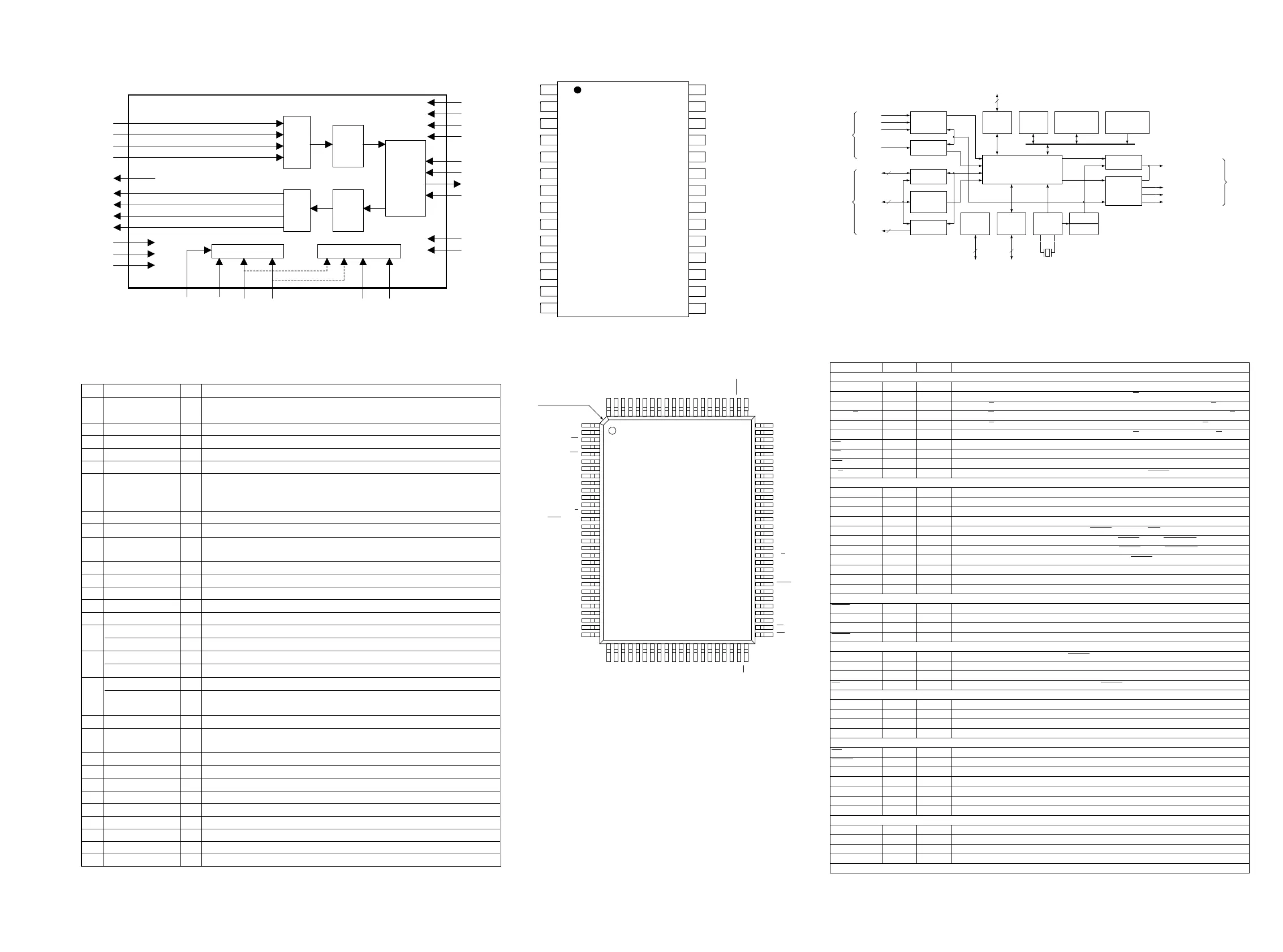
Pin 1 index mark,
notched corner, or both
ZR38601
(TOP VIEW)
1
30 51
80
100
31 50
81
AINL+
AINR+
VCOM
AOUTL+
AOUTL-
AOUTR-
AOUTR+
VREF
VA
AGND
CSN
(DIF)
CCLK
(CKS1)
CDTI
(CKS0)
P/S
MCLK
SDTI
SDTO
BICK
LRCK
DGND
VT
VD
ADC
DAC
HPF
DATT
SMUTE
Audio I/F
Controller
Control Register I/F Clock Divider
PDN
AINL-
AINR-
DEM1
DEM0
DFS
AGND
VCOM
AINR+
AINR-
AINL+
AINL-
VREF
VA
P/S
MCLK
LRCK
BICK
SDTO
SDTI CDTI(CKS0)
CCLK(CKS1)
CSN(DIF)
DFS
DEM1
VT
VD
DGND
AOUTL-
AOUTL+
AOUTR-
AOUTR+
PDN
DEM0
1
2
3
4
5
6
7
8
9
10
11
12
13
14 15
16
17
18
19
20
21
22
23
24
25
26
27
28
AK4528
Top
View
 Loading...