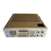
Do you have a question about the Marantz SR 8100DC and is the answer not in the manual?
Describes the composition of the frequency synthesizer system.
Details terminal connections and specifications for the MN1455LF microcomputer.
Lists and describes the terminal connections for the MN6147 PLL LSI.
Provides absolute maximum ratings for the MN6147 PLL LSI.
Illustrates the block diagram of the MN6147 PLL LSI.
Details the functions of each terminal on the MN6147 PLL LSI.
Details the switch and key matrix used for operations and functions.
Procedure for adjusting the DC offset of the set using a digital volt meter.
Procedure for adjusting the idling current using a digital volt meter.
Covers FM alignment, including LO, RF, stopping level, and stereo.
Procedures for AM RF and PLL oscillator alignment.
Schematic and component locations for the Tuner/Phono Amplifier board (P100).
Schematic and component locations for the Head Phone board (PW01).
Schematic and component locations for the Controller board (P500).
Schematic and component locations for the Main Amplifier board (P701).
Exploded view and parts list for the front panel assembly.
Exploded view and parts list for the top cover assembly.
Exploded view and parts list for the rear panel assembly.
Comprehensive list of electrical components used in the device.
| Total Harmonic Distortion | 0.05% |
|---|---|
| Damping Factor | 60 |
| Speaker Load Impedance | 4 - 16 ohms |
| Tuning Range | FM, MW |
| Power Output | 100 watts per channel (8 ohms) |