USB-1208LS User's Guide Functional Details
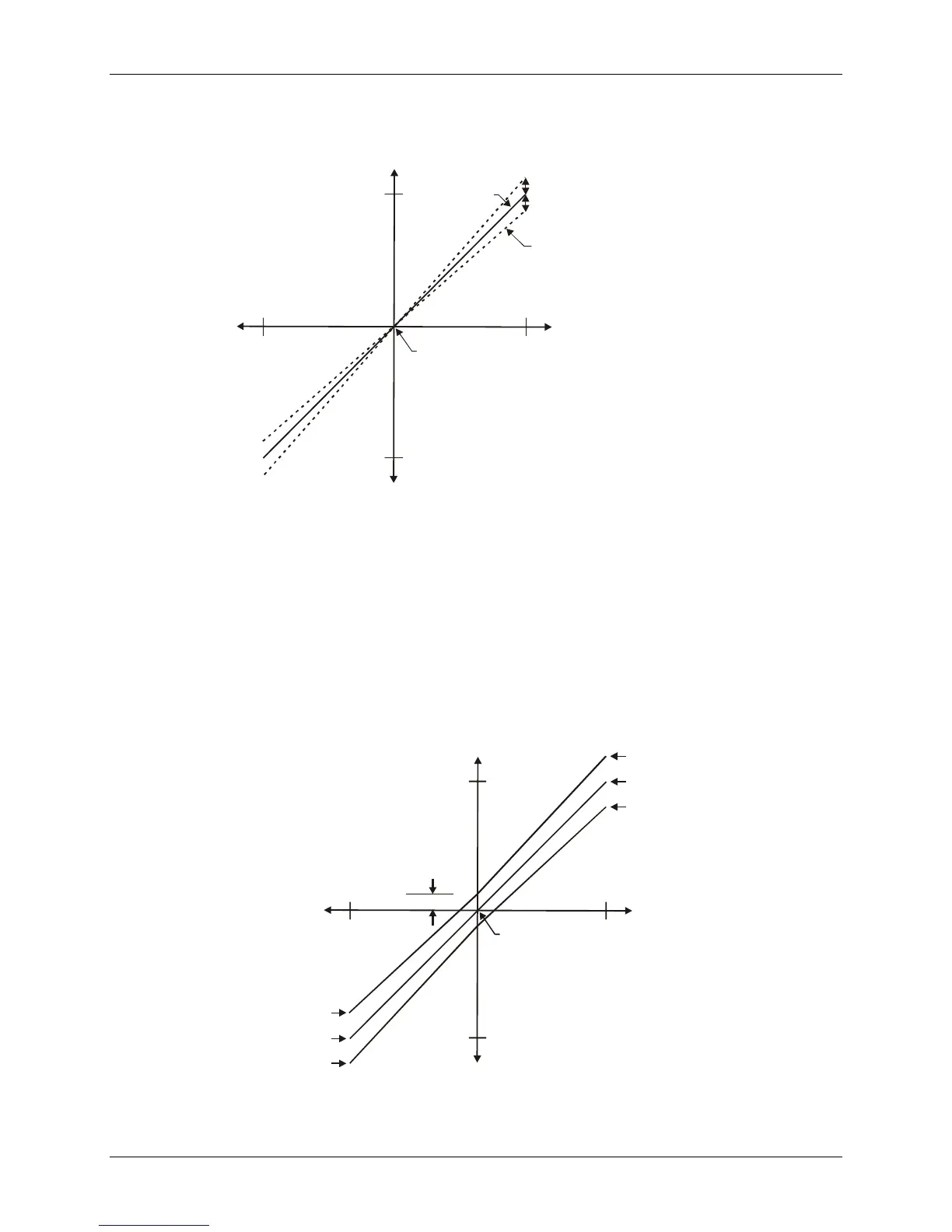
The accuracy plots in Figure 3-12 are drawn for clarity and are not drawn to scale.
-FS
+FS
Input Voltage
0
4095
Actual
Ideal
Output Code
Gain error=+0.2%, or +20 mV
Gain error=-0.2%, or -20 mV
2048
Figure 3-12. ADC Transfer function with gain error
For example, the USB-1208LS exhibits a typical calibrated gain error of ±0.2% on all ranges. For the ±10 V
range, this would yield 10 V × ±0.002 = ±20 mV. This means that at full scale, neglecting the effect of offset for
the moment, the measurement would be within 20 mV of the actual value. Note that gain error is expressed as a
ratio. Values near ±FS are more affected from an absolute voltage standpoint than are values near mid-scale,
which see little or no voltage error.
Combining these two error sources in , we have a plot of the error band of the USB-1208LS for the
±10 V range. This is a graphical version of the typical accuracy specification of the product.
Figure 3-13
Figure 3-13. Error band plot
The accuracy plots in Figure 3-13 are drawn for clarity and are not drawn to scale
-FS
+FS
Input Voltage
0
4095
9.77mV
2048
Output Code
Ideal
Ideal +9.77mV + 20 mVIdeal +9.77mV + 20 mV
Ideal -(9.77mV + 20 mV)
Ideal -(9.77mV + 20 mV)
Ideal
Ideal +9.77mV + 20 mV
3-11