Schematic Diagrams
B - 1
B.Schematic Diagrams
Appendix B: Schematic Diagrams
Table B - 1
SCHEMATIC
DIAGRAMS
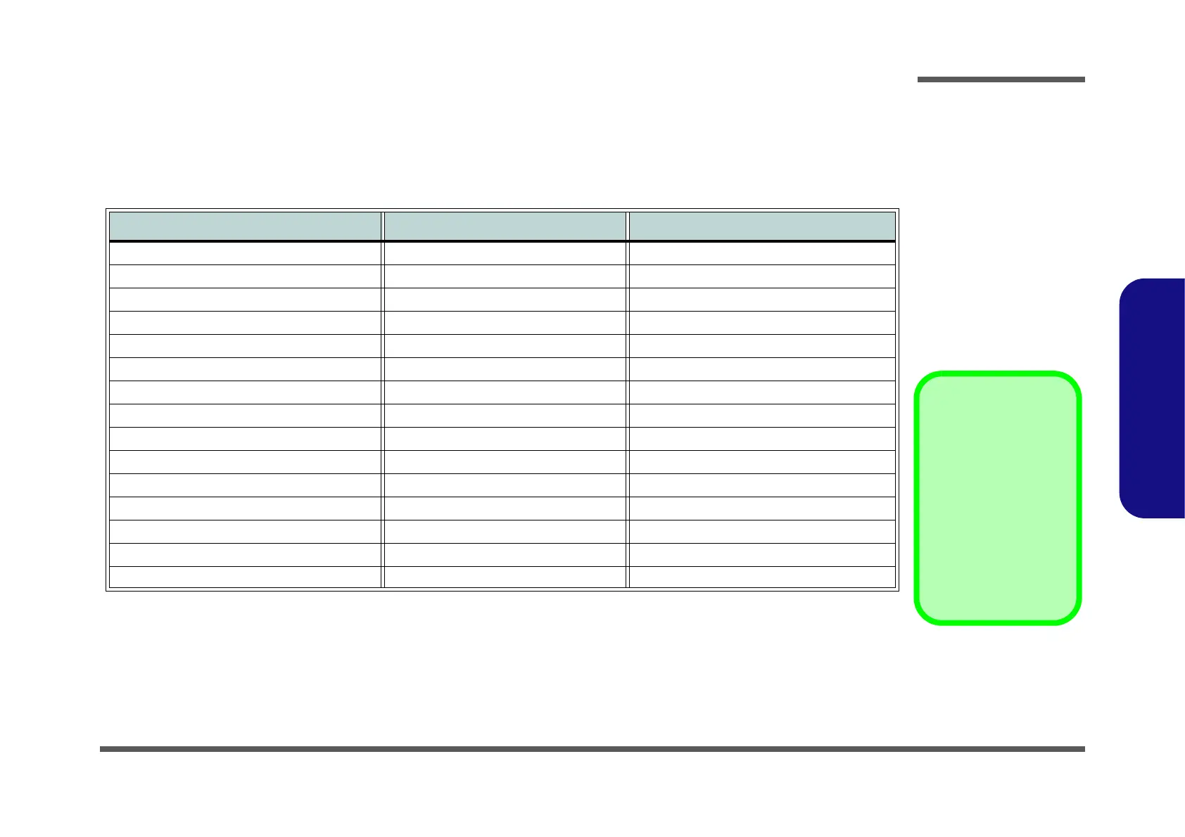
This appendix has circuit diagrams of the W950AU /W955AU notebook’s PCB’s. The following table indicates where
to find the appropriate schematic diagram.
Diagram - Page Diagram - Page Diagram - Page
System Block Diagram - Page B - 2 VGA PS8613 - Page B - 17 VCore - Page B - 32
Processor 1/7 - Page B - 3 LVDS PS8625 - Page B - 18 Charger, DC In - Page B - 33
Processor 2/7 - Page B - 4 USB Hub AU6259-JGF - Page B - 19 Audio Board - Page B - 34
Processor 3/7 - Page B - 5 Card Reader & LAN RTL8411B - Page B - 20 Audio Board - Page B - 35
Processor 4/7 - Page B - 6 HDMI, RJ45, Fan - Page B - 21 LID Switch Board - Page B - 36
Processor 5/7 - Page B - 7 WLAN, 3G, MSATA - Page B - 22 Power Switch Board - Page B - 37
Processor 6/7 - Page B - 8 Audio Codec ALC269 - Page B - 23 ODD Board - Page B - 38
Processor 7/7 - Page B - 9 USB 3.0, G-Sensor, TPM - Page B - 24 Power On Sequence - Page B - 39
Power 1 - Page B - 10 HDD, CCD, TPM, Power Con - Page B - 25
Power 2 - Page B - 11 CCD, MIC, LID, I/O Connector - Page B - 26
Power VSS - Page B - 12 HDD, ODD, LED - Page B - 27
RSVD - Page B - 13 System Power - Page B - 28
DDR3 SO-DIMM A - Page B - 14 VDD3, VDD5 - Page B - 29
DDR3 SO-DIMM B - Page B - 15 ALC269Q, VT1802S - Page B - 30
Panel, Inverter - Page B - 16 1.05V Series - Page B - 31
Version Note
The schematic dia-
grams in this chapter
are based upon ver-
sion 6-7P-W5S27-006.
If your mainboard (or
other boards) are a lat-
er version, please
check with the Service
Center for updated di-
agrams (if required).