5
5
4
4
3
3
2
2
1
1
D D
C C
B B
A A
Noe:
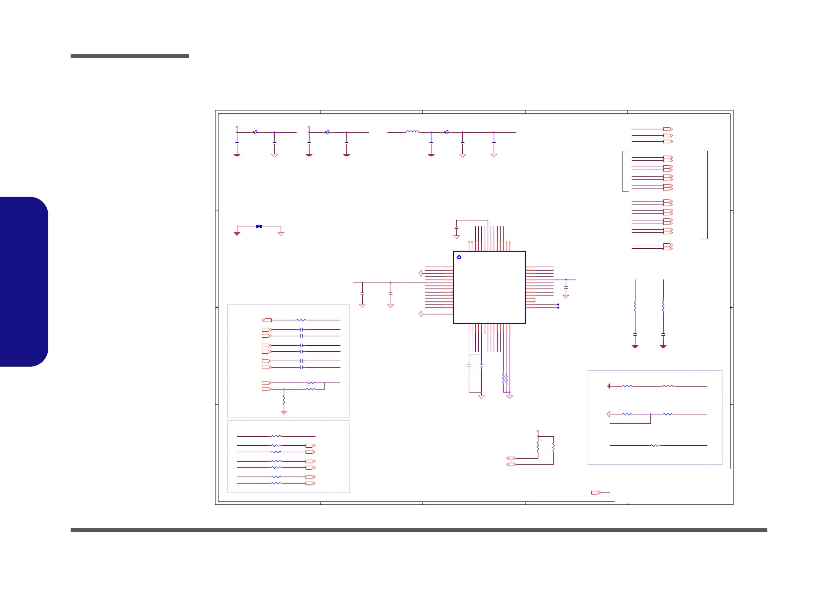
R13: LVDS output swing control
4.99K for default swing, change
the value for s wing adj us t
Note:
The decoupling caps shall be close
to the power pins as possible
1. Place the switching regulator inductor (L3) close to SW_OUT Pins (Pin15, Pin16).
2. The SW _OUT out put tr aces should be as wide as possible.
3. The GNDX pins (Pin17, Pin18) should be connected to the main PCB ground plane, with the device GND pins of the PS8625 connected to separate GND island (GNDA) for the device.
The GND is land (GNDA) s hould be c onnected to t he main GND plane (GND) with a single- point connec tion by use of a wide PCB tr ace.
4. Place the 4.7uF decoupling Capacitor (C4) for VDDIOX close to VDDIOX pin.
5. The GND of the 4.7uF capacitor (C4) for VDDIOX should be placed close to the GND of 4.7uF capacitor (C5) behind Inductor.
6. Place the bead (L2) for VDDIOX clos e to PS8625.
To LVDS Connector
Single link
LVDS
Dual link
LVDS
single PCB trace
6-03-08625-030
Power On Configuration
I2C_ADDR: I2C Slave address selection, internal pull-down ~80K
L: 0x10h~0x1Fh
H: 0x90h~0x9Fh
RLV_CFG: LVDS color depth and data mapping selection, internal pull-down ~80K
L: 8-bit LVDS, VESA mapping
M: 8-bit LVDS, JEIDA mapping
H: 6-bit LVDS, both VESA and JEIDA mapping
RLV_LNK: LVDS single link or dual link selection, internal pull-down ~80K
L: Single link LVDS
H: Dual link LVDS
Note:
The decoupling caps shall be close
to the power pins as possible
Note:
The decoupling caps shall be close
to the power pins as possible
Note:
The decoupling caps shall be close
to the power pins as possible
STUFF FOR LVDS
STUFF FOR EDP
LVDS-L1N
LVDS-L1P
LVDS-L2N
LVDS-L2P
LVDS-LCLKN
LVDS-LCLKP
LVDS-L0N
LVDS-L0P
LVDS-U1N
LVDS-U1P
LVDS-U2N
LVDS-U2P
LVDS-UCLKN
LVDS-UCLKP
LVDS-U0N
LVDS-U0P
VDDIO_LVDS
LVDS-U0N
LVDS-U0P
LVDS-U1N
LVDS-U1P
LVDS-U2N
LVDS-U2P
LVDS-UCLKP
LVDS_PLVDD_EN
P_DDC_DATA
LVDS-L0N
LVDS-L0P
LVDS-L1N
DRX0p
LVDS-L1P
VDDIO_LVDS
LVDS-L2P
DRX1p
DRX0n
DRX1n
RST#_LVDS
P_DDC_CLK
PD#_LVDS
EDP_HPD_R
VDDIOX_LVDS
VDDIOX_LVDS
LVDS-LCLKP
BRIGHTNESS_R
LVDS-LCLKN
VDD12
LVDS-L2N
VDDRX_LVDS
SW_OUT
SW_OUT
GND
GND
RLV_CFG
ENBLT
SMD_EDP_DAT
RLV_LNK/GPIO0
SMC_EDP_CLK
PWM_INREXT_LVDS
RLV_AMP
DAUXn
DAUXp
LVDS-UCLKN
VDDIOX_LVDS SW_OUT VDD12 VDDRX_LVDSVDDIO_LVDS
ENBLT
LVDS_PLVDD_EN
BRIGHTNESS_R
P_DDC_CLK
P_DDC_DATA
SMC_EDP_CLK
SMD_EDP_DAT
LVDS_PLVDD_EN VDDIO_LVDS
VDDIO_LVDS
RLV_LNK/GPIO0
RLV_CFG
VDDIO_LVDS
BRIGHTNESS_EDP PWM_IN
DAUXn
DAUXp
DRX0p
DRX0n
DRX1p
DRX1n
EDP_HPD_R
EDP_AUXN
EDP_AUXP
EDP_TXP_0
EDP_TXN_0
EDP_TXP_1
EDP_TXN_1
BRIGHTNESS_EDP BRIGHTNESS_R
EDP_TXN_0
EDP_TXP_0
EDP_TXN_1
EDP_TXP_1
EDP_AUXP
EDP_AUXN
VDDIO_LVDS
PD#_LVDS
RST#_LVDS
VDDIO_LVDS
GND_LVDS
GND_LVDS GND_LVDS
GND_LVDS
GND_LVDS
GND_LVDS GND_LVDS
GND_LVDS
GND_LVDS
GND_LVDS
GND_LVDS
3.3VS 3.3VS
3.3VS
GND_LVDS
GND_LVDS
LVDS-LCLKP 15
LVDS-U2P 15
LVDS-LCLKN 15
LVDS-U2N 15
LVDS-L2P 15
LVDS-U1P 15
LVDS-L2N 15
LVDS-U1N 15
LVDS-L0P 15
LVDS-L1P 15
LVDS-L0N 15
LVDS-L1N 15
LVDS-UCLKP 15
LVDS-U0P 15
LVDS-UCLKN 15
LVDS-U0N 15
LVDS_PLVDD_EN 15
ENBLT 15
BRIGHTNESS_R 15
P_DDC_DATA 15
P_DDC_CLK 15
SMD_EDP_DAT24
SMC_EDP_CLK24
3.3VS2,4,5,6,7,8,10,13,14,15,16,19,20,21,22,23,24,25,26,27,29,30,31
EDP_AUXP2
EDP_TXN_02
EDP_TXN_12
EDP_TXP_12
EDP_TXP_02
EDP_AUXN2
BRIGHTNESS_EDP8
BRIGHTNESS24
EDP_HPD8,15
DP_AUX# 15
DP_AUX 15
DP_TXN0 15
DP_TXP0 15
DP_TXN1 15
DP_TXP1 15
Title
Size Document Number Rev
Date: Sheet of
1.0
[17] LVDS_PS8625
Custom
17 39Tuesday, October 29, 2013
ᙔ!Ϻ!ႝ!တ!!DMFWP!DP/
6-7P-W 5S27-005
6-71-W5S20-D03
Title
Size Document Number Rev
Date: Sheet
of
1.0
[17] LVDS_PS8625
Custom
17 39Tuesday, October 29, 2013
ᙔ!Ϻ!ႝ!တ!!DMFWP!DP/
6-7P-W 5S27-005
6-71-W5S20-D03
Title
Size Document Number Rev
Date: Sheet
of
1.0
[17] LVDS_PS8625
Custom
17 39Tuesday, October 29, 2013
ᙔ!Ϻ!ႝ!တ!!DMFWP!DP/
6-7P-W 5S27-005
6-71-W5S20-D03
R558 *4.7K_04R558 *4.7K_04R553
4.7K_04
R553
4.7K_04
R556 *0_04R556 *0_04
R554 *4.7K_04R554 *4.7K_04
C466
0.01u_16V_X7R_04
C466
0.01u_16V_X7R_04
R545 4.99K_1%_04R545 4.99K_1%_04
C468 0.1u_10V_X7R_04C468 0.1u_10V_X7R_04
C467 0.1u_10V_X7R_04C467 0.1u_10V_X7R_04
C452
0.47u_10V_Y5V_04
C452
0.47u_10V_Y5V_04
C462 0.1u_10V_X7R_04C462 0.1u_10V_X7R_04
R567 0_04R567 0_04
C465
0.1u_16V_Y5V_04
C465
0.1u_16V_Y5V_04
R542 1K_04R542 1K_04
C457
*4.7u_6.3V_X5R_06
C457
*4.7u_6.3V_X5R_06
R561
*28mil_06
R561
*28mil_06
R557 *4.7K_04R557 *4.7K_04
C454
0.47u_10V_Y5V_04
C454
0.47u_10V_Y5V_04
C469 0.1u_10V_X7R_04C469 0.1u_10V_X7R_04
R543 4.99K_1%_04R543 4.99K_1%_04
R552
4.7K_04
R552
4.7K_04
C460
2.2u_6.3V_X5R_04
C460
2.2u_6.3V_X5R_04
L64
HCB1005KF-121T20
L64
HCB1005KF-121T20
R555 *0_04R555 *0_04
R540
10K_04
R540
10K_04
R568 *0_04R568 *0_04
R546 *0_04R546 *0_04
C463
0.1u_16V_Y5V_04
C463
0.1u_16V_Y5V_04
C459
1u_6.3V_X5R_04
C459
1u_6.3V_X5R_04
C458
1u_6.3V_X5R_04
C458
1u_6.3V_X5R_04
R16 *0_04R16 *0_04
C470 0.1u_10V_X7R_04C470 0.1u_10V_X7R_04
R541
10K_04
R541
10K_04
C455
4.7u_6.3V_X5R_06
C455
4.7u_6.3V_X5R_06
L62
HCB1005KF-121T20
L62
HCB1005KF-121T20
C456
4.7u_6.3V_X5R_06
C456
4.7u_6.3V_X5R_06
C464 0.1u_10V_X7R_04C464 0.1u_10V_X7R_04
R549 4.7K_04R549 4.7K_04
C461
0.1u_16V_Y5V_04
C461
0.1u_16V_Y5V_04
L61
HCB1005KF-121T20
L61
HCB1005KF-121T20
R551 *0_04R551 *0_04
C471
0.01u_16V_X7R_04
C471
0.01u_16V_X7R_04
R548 *4.7K_04R548 *4.7K_04
R550 *0_04R550 *0_04
L63
BCNR3010C-2R2M
L63
BCNR3010C-2R2M
1 2
C453
1u_6.3V_X5R_04
C453
1u_6.3V_X5R_04
R544
*100K_04
R544
*100K_04
U13
PS8625
U13
PS8625
SW_OUT
15
SW_OUT
16
GNDX
17
GNDX
18
VDD12
19
TESTMODE
20
RLV_LNK/GPIO0
21
RLV_CFG
22
ENBLT
23
CSDA/MSDA
24
CSCL/MSCL
25
REXT
26
BLV_AMP
27
GND
28
TA1n
42
TA1p
41
TB1n
40
TB1p
39
VDDIO
38
TC1n
37
TC1p
36
TCK1n
35
TCK1p
34
ENPVCC/I2C_ADDR
33
TD1n
32
TD1p
31
DDC_SDA
30
DDC_SCL
29
NC
56
NC
55
TA0n
54
TA0p
53
TB0n
52
TB0p
51
VDDIO
50
TC0n
49
TC0p
48
TCK0n
47
TCK0p
46
PWMI
45
TD0n
44
TD0p
43
DAUXn
1
DAUXp
2
GND
3
DRX0p
4
DRX0n
5
VDDRX
6
DRX1p
7
DRX1n
8
RST#
9
PD#
10
HPD
11
PWMO
12
VDDIOX
13
VDDIOX
14
Epad
57
C472
0.1u_16V_Y5V_04
C472
0.1u_16V_Y5V_04
R547 *0_04R547 *0_04