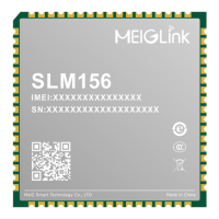
MeiG_SLM156_Hardware Design Manual
MeiG Smart Technology Co., Ltd
Contents
Important Notice ....................................................................................................................................... 1
Revision History ....................................................................................................................................... 2
Contents .................................................................................................................................................... 3
Table Index ................................................................................................................................................ 5
Figure Index .............................................................................................................................................. 6
1 Introduction ........................................................................................................................................ 7
1.1 Safety Instructions .................................................................................................................... 8
1.2 Purpose of the Document ........................................................................................................ 9
1.3 List of Contents ........................................................................................................................ 9
2 Product Overview ............................................................................................................................ 10
2.1 Basic Description ................................................................................................................... 10
2.2 Main Performance .................................................................................................................. 10
2.3 Evaluation Board .................................................................................................................... 13
3 Application Interface ....................................................................................................................... 14
3.1 General Description ............................................................................................................... 14
3.2 Pin Definition of LCC Module ................................................................................................. 15
3.3 Pin Description ....................................................................................................................... 16
3.4 Operating Mode ..................................................................................................................... 21
3.5 Power Saving ......................................................................................................................... 22
3.5.1 Flight Mode .................................................................................................................. 22
3.5.2 Power Saving Mode (PSM) ......................................................................................... 23
3.5.3 Extent Idle Mode Discontinuous Receiving ................................................................ 23
3.6 Power Supply ......................................................................................................................... 24
3.6.1 Power Supply Pins ...................................................................................................... 24
3.6.2 Decrease Voltage Drop ............................................................................................... 25
3.6.3 VDD_EXT Voltage Output........................................................................................... 25
3.7 Turn on and off ....................................................................................................................... 26
3.7.1 Turn on Module Using the POWER_ON/OFF ............................................................ 26
3.7.2 Turn off Module Using the POWER_ON/OFF Pin ...................................................... 28
3.8 Reset Fuction ......................................................................................................................... 28
3.8.1 AT Command Reset .................................................................................................... 28
3.9 USIM/SIM Interface ................................................................................................................ 28
3.9.1 USIM/SIM Card Interface Pin Description .................................................................. 29
3.10 USB Interface ......................................................................................................................... 31
3.10.1 USB Pin Description .................................................................................................... 31
3.10.2 USB Reference Circuit ................................................................................................ 31
3.10.3 USB Driver .................................................................................................................. 32
3.11 UART Interface ....................................................................................................................... 32
3.11.1 UART Pin Description ................................................................................................. 33
3.12 Network Status Indication ...................................................................................................... 34
3.13 Status Indicaiton ..................................................................................................................... 35
3.14 ADC Function ......................................................................................................................... 36
3.15 DLOAD Interface .................................................................................................................... 37