P341/EN AD/F43 Update Documentation
(AD) -44
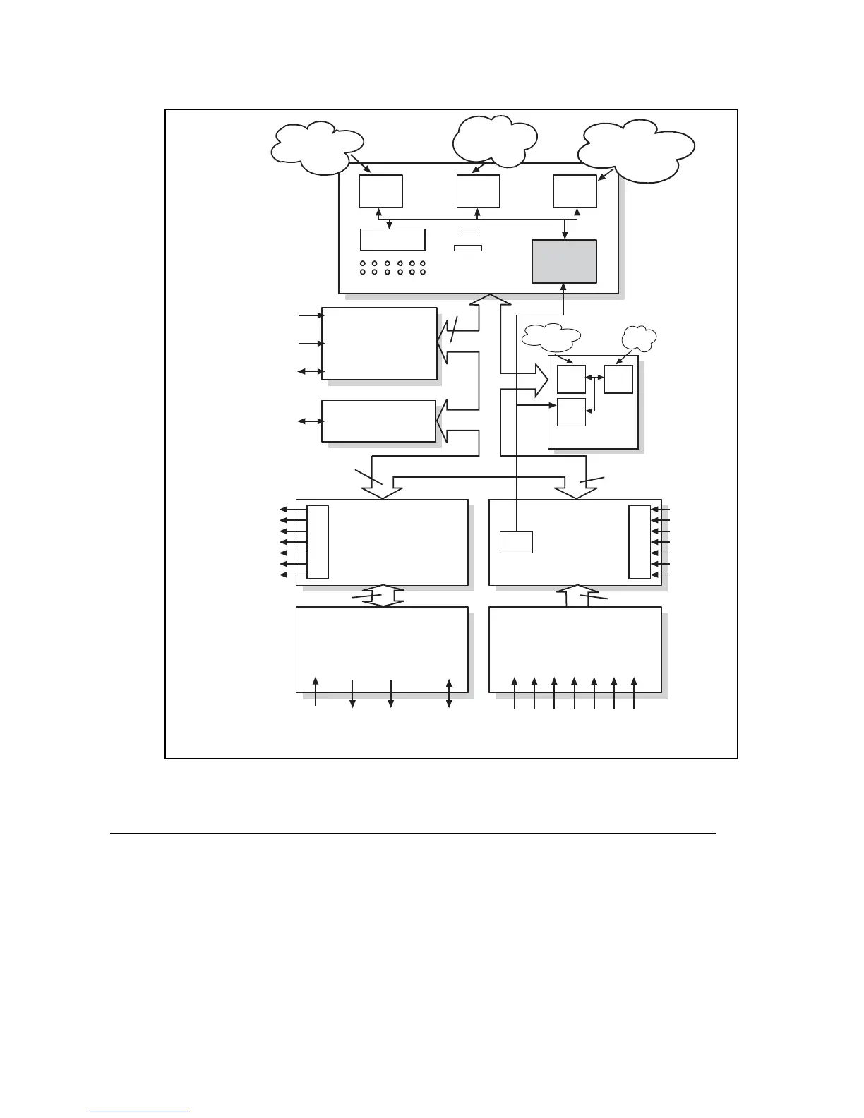
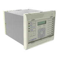
MiCOM P341
Main processor board
Relay board
Power supply board Transformer board
Input
board
Parallel data bus
Flash
EPROM
CPU
EIA(RS)232 Front comms port
Parallel test port
Current & voltage inputs
Digital inputs
Power
supply
Rear EIA(RS)485
communication port
Output relay contacts
ADC
Output relays
Opto-isolated
inputs
Analogue input signals
Power supply (3 voltages),
rear comms data
Digital input values
Power supply, rear comms
data, output relay status
Timing data
Watchdog
contacts
Field
voltage
P0126ENd
Default settings & parameters,
language text, software code.
Present values of all settings.
Front LCD panel
LEDs
Alarm, event, fault,
disturbance &
maintenance
records
Battery
backed-up
SRAM
Executable software
code & data, setting
database data
SRAM
Ethernet comms
2nd rear comms port EIA(RS)485
optional
Fibre optic rear comms port
optional
IRIG-B and/or 2nd rear comms board
(where fitted)
IRIG-B and/or FO rear port, or
IRIG-B signal
optional
Ethernet board
(where fitted)
Comms between
main & coprocessor
boards
CPU code
& data
FPGA
CPU
SRAM
Coprocessor board
(where fitted)
Serial data bus
(sample data)
Figure 1: Relay modules and information flow
2.4.3 High break relay board
One ‘high break’ output relay board consisting of four normally open output contacts is
available for the P341 as an option.
This board contains a hybrid of MOSFET solid state devices (SSD) in parallel with high
capacity relay output contacts. The MOSFET has a varistor across it to provide protection
which is required when switching off inductive loads as the stored energy in the inductor
causes a reverse high voltage which could damage the MOSFET.