dsPIC33/PIC24 Family Reference Manual
DS30009711C-page 14 2006-2019 Microchip Technology Inc.
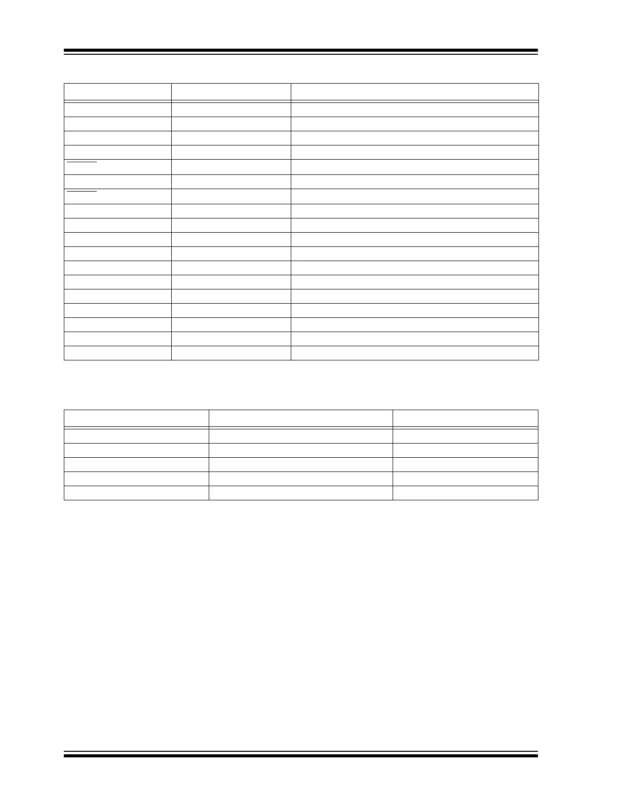
Table 4-1: Output Selection for Remappable Pin (RPn)
Table 4-2: Registers Associated with Output Function on RPn Pin
4.3.3 MAPPING LIMITATIONS
The control schema of peripheral select pins is not limited to a small range of fixed peripheral
configurations. There are no mutual or hardware enforced lockouts between any of the peripheral
mapping SFRs; literally any combination of peripheral mappings across any or all of the RPn pins
is possible. This includes both many-to-one and one-to-many mappings of peripheral inputs and
outputs to pins. While such mappings may be technically possible from a configuration point of
view, the user must ensure the selected configurations are supportable from an electrical point
of view.
Function
(1)
RPnR<5:0> Output Name
NULL 0 The pin is an I/O Port pin.
C1OUT 1 RPn tied to Comparator 1 Output.
C2OUT 2 RPn tied to Comparator 2 Output.
U1TX 3 RPn tied to UART1 Transmit.
U1RTS
4 RPn tied to UART1 Ready-to-Send.
U2TX 5 RPn tied to UART2 Transmit.
U2RTS
6 RPn tied to UART2 Ready-to-Send.
SDO1 7 RPn tied to SPI1 Data Output.
SCK1OUT 8 RPn tied to SPI1 Clock Output.
SS1OUT 9 RPn tied to SPI1 Slave Select Output.
SDO2 10 RPn tied to SPI2 Data Output.
SCK2OUT 11 RPn tied to SPI2 Clock Output.
SS2OUT 12 RPn tied to SPI2 Slave Select Output.
OC1 18 RPn tied to Output Compare 1.
OC2 19 RPn tied to Output Compare 2.
OC3 20 RPn tied to Output Compare 3.
OC4 21 RPn tied to Output Compare 4.
OC5 22 RPn tied to Output Compare 5.
Note 1: The device may have more or less number of output functions. For actual details, please refer to the
specific device data sheet.
Pin Register Associated bits
RP0 RPO0<5:0> RP0R<5:0>
RP1 RPO0<13:8> RP1R<5:0>
RP2 RPO1<5:0> RP2R<5:0>
RPn RPOn/2<5:0> RPnR<5:0>
RPn + 1 RPOn/2<13:8> RPn + 1R<5:0>
Legend: n = 0, 2, 4, . . . , etc.